PDP-11/45: ECOs
Sun 07 June 2020 by Fritz Mueller[A catch-up article, documenting discoveries of Jan/Feb 2019 and some additional research while writing up.]
Okay, per last article, specifics of parity-handling on my CPU indicate that it is missing several significant ECOs. I spent some time seeing if I could dig up and/or puzzle out more details on ECOs issued for the CPU, MMU, FPU, chassis, power supplies, and peripherals. What I could find I will summarize here.
ECO Designations
This material is excerpted from PDP-8E_ECO_LOG_Dec74.pdf on bitsavers. Of particular note is the distinction between "ECOs", implemented at the factory, and "FCOs", designed to be implemented in the field. The latter are distinguishable by the presence of an additional letter inserted in their identifier:
ECO IDENTIFIER
Every ECO that is issued for a product is entered in the DEC-O-LOG with an identification number that includes the equipment type or option number, followed by a unique sequential number. For example, the ECO identifier “LA30-00053" is assigned to the 53rd ECO issued for the LA30 DECwriter.
FIELD DISTRIBUTION
Depending upon the nature of the engineering change, ECOs are categorized in one of five groups, which are assigned letter codes F, D, DF, P, and M. The appropriate field distribution code for the ECO appears on the first line of the DEC-O-LOG entry.
F Code: When the ECO has been engineered for field retrofit, it is coded “F”. A Field Change Order (FCO) is prepared by Field Service. The FCO provides a complete description of the engineering change and includes instructions for making the change to existing equipment installations.
When an F-coded ECO is issued, a letter code is inserted as the first character of the sequential ECO identifier number. The letter code indicates the level of urgency or importance of the ECO as follows:
A   Mandatory change - highest priority      D   Low Priority change
B   Mandatory change                         E   Optional change for product improvement
C   Mandatory change if specified
    trouble symptoms are observed
NOTEAll ECOs issued for a product are entered into the DEC-O-LOG. Usually, the publication process that produces updated DEC-O-LOG pages is triggered by an F-coded ECO. At that time, any D, DF, P, or M-coded ECOs that precede the latest FCO are also published to provide a complete history of all ECO activity for the product.
D Code: An ECO that changes the design of an equipment in production is coded “D”. This category includes changes to:
Production models, as a normal step in the design phase of a new product.
All future production units of a specific equipment type or option, and the ECO is not to be retrofitted.
Production units that include special features ordered by a specific customer.
ECOs that are coded “D” are not retrofitted into existing units installed in the field. They are entered in the DEC-O-LOG for information purposes, and customers can purchase them from DEC.
DF Code: The “DF" field distribution code is assigned to ECOs that change the design of products that have been released to the field in limited quantity, when the retrofit is essentially a part of the design process.
P Code: When an ECO is issued solely for the purpose of changing engineering drawings or other engineering documentation, it is coded P (for Prints).
M Code: When an ECO is issued to change mechanical parts, structural components, or other items that do not affect existing units in the field, it is coded "M". M-coded ECOs cannot be purchased for retrofit.
ML, DD, and WL REVISIONS
A Master Drawing List (ML) or a Drawing Directory (DD) lists all engineering drawings included in the engineering drawing set for a specific product or option. If an ECO causes any drawing in that set to be revised, the ML or DD is revised to indicate the latest revisions of all drawings in the set. The revision code for the ML or DD that reflects the ECO is included in the first line of that ECO entry in the DEC-O-LOG.
A Wire List (WL) is used to indicate all wired connections for an equipment or option System Unit. If an ECO calls for changes in this wiring, the WL is appropriately revised. The revision code for the WL that reflects the ECO is included in the first line of that ECO entry in the DEC-O-LOG.
DEC-O-LOGs on Bitsavers
Unfortunately, at time of writing the selection of DEC-O-LOGs archived at bitsavers (here) is pretty sparse with respect to the '11/45. There is a 1974 log for the M8105 TMC CPU board, a 1973 log for the M8108 SSR MMU board, and that's pretty much it for the '11/45 :-(
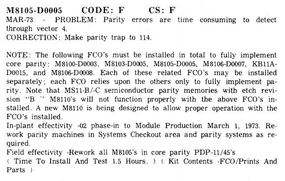
Here's an entry from the M8105 log that is found there, relating to the subject of the previous article:

Unfortunately, no cut/jump list here (some log entries do contain these). There is a bunch of useful info to be gleaned, though:
-
The complete trap parity to 114 mod involved all of the M8100 (DAP), M8103 (RAC), M8105 (TMC), M8106 (UBC) boards, plus mods to the processor wire-wrap backplane.
-
All of these FCOs are given prefix "D", meaning DEC viewed fixing these in the field as "low priority".
-
A reason for the change is given: "Parity errors are time consuming to detect..." I suppose what they mean is that adding code to sniff for possible parity errors, in order to distinguish these from other possible sources of trap 4, was getting in the way of handling the other trap 4 sources promptly. I can't see that there would be any difference in processor overhead per se in dispatching between vector 4 and vector 114?
-
Machines which would trap parity to 114 as-delivered were phased into production starting in March 1973. This is consistent with the low serial number and component date codes in my machine, confirming its manufacture somewhere in 1972.
-
The note about the MS11-B/C (M8110 SMC) is also interesting, in conjunction with fact that the re-work is called out for "all core-parity PDP-11/45's".
PDP-11/45 11/50 MOS Memory Troubleshooting Guide
As it turns out, this document is a bit of a gold mine, containing a complete list of ECO's for the '11/45 CPU/MMU/FPU modules, console, and backplane, as of 1974. There are brief notes, dates, and revision codes for each.
In the case of the M8105, we can compare this with the DEC-O-LOG we do have on bitsavers. This shows that the "Notes" in the troubleshooting guide in some cases give information not included in the corresponding DEC-O-LOG entries. For example, the DEC-O-LOG entry for M8105-00002 says only:
Change disable gate in priority arbitration.
...while the troubleshooting guide offers a bit more explanation:
Corrects FP TRAPS to location 4 where BRs below 7 occur at the same time.
The troubleshooting guide also calls out several "clusters" of interdependent ECOs:
-
Parity, as remarked above: M8100-00003, M8103-00005, M8105-00005, M8106-00007/00008/00012/00012A, KB11-A-00015, and M8110-00018.
Separately, M8106-00003, from August 1972, is annotated "Adds disable jumper for UNIBUS PARITY", as observed missing in my hardware in the previous article.
-
CMP.B, BIT.B: M8100-00002A, KB11-A-00006. These are dated June, 1972. Hmm, I should check these instructions on my machine...
-
Speed-up: M8104-00002, M8106-00005A, KB11-A-00012A/00013. Not sure what is "sped up" here, but perhaps Unibus signaling; the M8106 change is annotated "Clear MSYN with T1".
Also of note are a few items that seem to relate directly to previously observed behaviors of my machine:
-
KM11 uPB: M8109-00015 "CPU fails to halt on selected ROM state when micro program break mode is set on maintenance card. Detected when running a test sequence not containing a pause, i.e., 150ns cycle time." Ah ha! I had run across this (mis)behavior previously, noted here.
-
Slots 26-28: KB11-A-0008 "Signal missing in small peripheral controller slots in KB11-A (slots 26-28)." Another ah ha... This seems likely related to issues noted here.
-
Burnt +5V Trace: KB11-00001: "Reworks backpanels with 24 AWG wire in parallel with +5 V etch." This may explain the burnt trace and "extra red wire" as noted here.
Jay Jaeger DEC-O-LOG Microfiche Transcriptions
After an ask on the cctalk mailing list, Jay Jaeger commented that he has some complete sets of DEC-O-LOGs on microfiche! Though he has no equipment with which to scan fiche, he very kindly took the time to manually transcribe those that seemed like they might be of most interest to me (thanks, Jay!) Jay has made his transcriptions publicly available here, under pdf/dec/fieldService/dec-o-log.
There is a lot there, and it's worth a read. Here are some excerpts I found relevant to discussions and investigations here:
-
On the parity rework:
M8100-C0003 CODE: F CS C Etch C JAN-73 [FCO]
Problem: Parity errors require the generation of trap vector 114
Correction: Modify trap vector logic
Required on all 11/45 systems with parityM8103-C0005 CODE: F CS F MAR-73 [FCO]
Problem: Parity errors need special abort logic to assert ZAP signal
Correction: Modify ZAP gate on RACAM8105-D0005 CODE: F CS F MAR-73 [FCO]
Parity errors are time consuming to detect through vector 4. Core parity requires these changes: M8100-D0003, M8103-D0005, M8105-D0005, M8106-D0007, KB11A-D0015 and M8106-D0008
FCO's may be installed separately - each FCO relies upon the others only to fully implement parity.
NOTE: MS11-B/C semiconductor parity memories with etch revision B M8110s will NOT function properly with these FCOs. A new M8110 is being designed to function with these FCOs.
M8106-D0007 CODE: F CS: J [FCO]
Problem: Parity errors are time consuming to detect through vector 4
Correction Allow processor to trap to 114 for parity errors.M8106-D0008 CODE: F CS: K MAR-73 [FCO]
Problem: UNIBUS parity errors cause machine to halt
Correction: Disable UBCB UNI PERF [ 1 ] L from generating UBCB PARITY ERR SET L.M8106-C0012 CODE: F CS: M JUN-73 [FCO]
Problem: MOS Parity memory is too tight
Correction: Strobe parity errors sooner
NOTE: See M8106-C0012ARework in parity systems with M7259 or etch revision C M8110s, rework all systems with parity and all PDP11-45s at next PM.
M8106-C0012A CODE: F JUN-73 [FCO]
The rework procedure in M8106-C0012 in steps #25 and #26 incorrectly references an R22. Should be R20.
KB11A-D0015 CODE: F DD:M WL:L [FCO] MAR-73
Problem: Detection of parity errors through vector 4 is slow.
Correction: Detect parity errors through vector 114.Wire Adds: D11D2 to A06P1, E12A1 to F11F1, C09K1 to E12A1
NOTE: This FCO must be installed in conjunction with the following FCOs to implement core parity: M8100-D0003, M8103-D0005, M8106-D0007 and M8106-D0008. Each of these related FCOs may be installed separately.
Note that MS11-B/C semiconductor parity memories with etch revision B M8110s will NOT function properly when above FCOs are installed. A new M8110 is being designed to function with these FCOs.
Okay, much of this confirms deductions worked out in the previous article. The big additional clue here is that we actually have the backplane wire adds this time!
-
D11D2 to A06P1: This forwards UBCB PARITY ERR L, already at the TMC card, on to DAPE E7. This provides parity condition input to the extended trap vector generation logic explored in the previous article.
-
E12A1 to F11F1 and C09K1 to E12A1: These relate to enhanced abort processing -- they distribute UBCB PE ABORT L to TMCC E87, TMCE E38, and RACA E52, which I have not previously inspected.
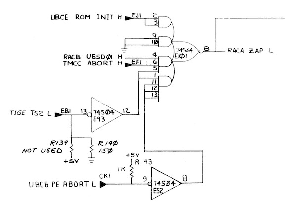
Looking at the RAC changes first, we have this:

...which, per expectation, is not implemented on the RAC board I am running; no connection from CK1 to E52, and no connection from E52 to E101. The ZAP signal is used to force the microcode counter to 200 on a trap or on power up, kicking off the exception handling microcode flow on sheet FLOWS 12. I'm not sure why parity required special plumbing here; by my read a parity error should end up setting TMCC ABORT H which should also result in a ZAP?. My guess would be the special plumbing allows the trap to be taken at an earlier clock phase?
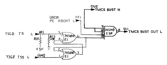
On the TMC we have these:


Also related to abort signaling, and also not implemented on my machine (no connection from FF1 to E87 or E38, pins 12 and 10 common on E38). So perhaps the reason to move parity to its own trap vector wasn't to avoid extra discrimintation logic in the trap 4 handler, but rather to enable an accelerated abort path without affecting extablished behavior of the other machine exceptions on vector 4? Curious...
-
-
On CMP.B, BIT.B:
M8100-A002A CODE: DF JUN-72 [FCO]
Problem: Disposition code on M8100-A0002 is 02: phase-in
Correction: Change to code 03: rework immediately.
Problem: CMP.B and BIT.B instructions with SM0 and DM0 and DF7 will destroy the PC
Correction: Inhibit PCB clock under those conditionsThe troubleshooting guide mentions that that this change also needs KB11-A-00006, but that is not included in Jay's transcript (bummer).
In any case, the description here tells us a lot more about the exact nature of the bug.
SM0,DM0,DF7here are microcode conditions; collectively this description implicates a CMP or BIT instruction, either byte or word length, with two registers as arguments, and the second argument being the PC (R7).CMP or BIT should not modify their second argument, but inspection of the the microcode flows shows that under this particular set of conditions the flow (
FET.00,FET.10,IRD.00,EXC.90) is shared with many other E/class instructions which should do. So an update inhibit derived from existing microcode outputs to distinguish this particular set of conditions is needed, and thus this FCO.Here again the schematics hold some clues. The relevant bit is the net for CLKPCB H on drawing DAPJ:

The AND terms of E42 serve as inhibits for the update signal, which otherwise sources from TIGC T1 H via E43. The top three terms in the diagram inhibit on cases of
UPCB=2 * ~SF7,UPCB=0, orUPCB=3 * ~DF7(with some term elimination on the first case). This would be the vanilla implementation of the UPCB microcode signals.The bottom-most AND term seems to be the one involved in the FCO. This adds an additional inhibit,
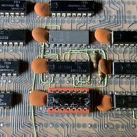
UPCB=3 * ICLASS * UPWE, which would be active in the situation described in the FCO description. Some minor additional clues here are that the handwriting for the signal names here doesn't quite match the rest of the drawing and that the backplane pin assignment for bringing in UPWE00 is not contiguous with the others in this net; together these suggest revision. From this we could also guess that the missing corresponding KB11-A-00006 probably involves bringing signal RACB UPWE00 H to pin E06V2.Inspection of my DAP modules shows the predicted changes implemented around E42 with green-wires, so it looks like my machine did get this FCO, either in the factory or the field:

Next time I have the machine fired up I'll experiment with some BIT instructions from the front panel and make sure.
-
On the "speedup" fixes:
M8106-A0005 CODE: F CS: F DEC-72 [FCO]
Problem: Present board not meeting cycle time specifications for UNIBUS.
Correction: Add logic changes.
NOTE: This FCO must be installed in conjunction with FCO KB11A-A0012M8106-A005A CODE: F JAN-73 [FCO]
Problem 1: Rework procedure in M8106-A0005 is incorrect.
Correction 1:
In step #2 changed E83-11 to E83-13
In step #4 change R23 to R22
Problem 2: The assembly hole drawing does not specify which side of the board etch cut #13 is on
Correction 2: Side 2KB11A-A0012 CODE: F DD: J WL: J DEC-72 [FCO]
Problem: 11/45 processor does not meet UNIBUS cycle time specification.
Correction: Correct KB11-A back panel attached ADD/DELETE sheet and install FCO M8106-A0005 to UBC module.KB11A-A012A CODE: F DEC-72 [FCO]
Problem: Not all the add/deletes listed on sheet 2 of KB11A-A0012 are necessary for this retrofit.
Correction: use the ADD/DELETE sheet included in this supplement for FCO KB11A-A0012.KB11A-E0013 CODE: F DD: K WL: K JAN-73 [FCO]
Problem: Improve performance of PDP-11/45 processor as UNIBUS master.
Correction: Revise KB11-A Wire List as defined the ADD/DELETE sheet and install etch revision C M8104 moduleNOTE: This FCO completes the total FCO package necessary for improving the speed performance of the PDP-11/45 with core memory. Note prerequisite FCOs are KB11A-A0012, KB11A-A012A and M8106-A0005.
Well, definitely Unibus timing related then. There is not very much info to start from here, and logs for the M8104 module are also missing from Jay's transcripts (perhaps not issued since no F-coded ECOs for this board?)
We do see from above, though:
- Involvement of M8106 E83 (sheet UBCB, driving CLR DESKEW L). Handwriting and "white out" artifacts around this gate on the engineering drawings also suggest rework.
- Involvement of M8106 R22 (also sheet UBCB, pull up on fastbus parity error handling)
- The troubleshooting guide annotates M8106 00005 "CLR MSYN with T1". Handwriting mismatch on the clock input of the MSYN flip-flop (sheet UBCB, E79) may be related.
- At least 13 etch cuts existed in the FCO (!)
Looking through the drawings a bit more here after this, I noticed for the first time (doh!) that there is an updated set of Unibus timing diagrams explicitly to be used with M8104 rev C and post- KB11-A-E00013. The differences seem to be around the bus long pause cycle. This prompted another look through the 1972 and 1976 KB11-A maintenance manual, and sure enough, in section 8.7.2 of the 1976 version we find:
ECO KBl l-A No. 13 ("Speed-up ECO"), in conjunction with Revision C or higher of the PDR Module (M8104), has changed the data transfer operations. Explanations of both versions are presented in this paragraph. (In general, ECO KB11-A No. 13 eliminated the bus long pause cycle.)
...followed by much description of the signalling differences between pre- and post- KB11-A-E00013 machines. This can definitely be mined for further clues.
I did verify that at least some of this rework is not implemented on my M8106 boards (specifically, configuration of E83 on my boards does not match either of the apparent revisions in the drawings). Definitely a lot more work to do puzzling this one out. Even though I'll continue to investigate the details of this change, it probably ends up being too much to undertake without complete documentation.
-
On KM11 uPB Break:
M8019-C0015 CODE: F CS: R CS: M3 APR-74 [FCO]
Problem: CPU fails to halt on selected ROM state when Micro Program break mode is set on maintenance card. The problem is detected when running a test sequence not containing a pause 150 nsec cycle time. Correction: Delete U/L: CTRL latch flipflop and add latch at input gating. Test by running a branch dot with ROM match at 343.
FOR ETCH REVISION C:
Cuts:
Side 2 at E12 pin 9
Side 2 E32 pin 9 to E31 pin 13
Side 2 E32 pin 9 to E32 pin 10
Side 2 at E42 pin 13
Remove jumper E22 pin 14 to E35 pin 7Jumpers:
E12 pin 9 to E22 pin 11
E42 pin 13 to E35 pin 7
E42 pin 8 to E32 pin 9
E32 pin 10 to E31 pin 13(etch revision F instructions ellided; in Jay's transcript linked above)
NOTE: Etch revision F boards are reworked from CS revision P to R. Etch revision C boards are reworked from CS revision M2 to M3.
My M8109 timing generator is etch C. There are a lot of ECOs on this board, culminating in CS level M2 ahead of this FCO. In principle, many/most of these are verifiable by inspection, based on information contained in Jay's transcripts.
This one is a bit deep, and I haven't really covered much about the M8109 yet. I'll probably take up analysis of this problem, the associated FCO fix, and inspection/determination of the revision level of my board as its own topic in a future article. I'd like to implement this fix if it proves not overly complicated.
-
On slots 26-28:
KB11A-B0008 CODE: DF DD: E WL: E SEP-72 [FCO]
Problem: Small peripheral controller slots in KB11-A panel, slots 26 thru 28, are not wired to accept some quad module controllers: NPG, PA, PB, LTC, ACLO, DCLO and +15V are missing. Correction: Revise wiring to include signals listed above.
Wow, lots missing from these slots besides the +15V and NPG I had noticed. In other correspondence, Jay mentions that the DL11 (with which I was having trouble in these slots) is explicitly mentioned elsewhere in this FCO.
-
On the burnt-trace / extra wire situation:
KB11-00001 CODE: D May-72 [ECO]
Problem: Etch carrying +5V current from Mate-n-Lock pins to backpanel pins is not heavy enough to carry required current. Correction: Run 24AWG wire in parallel with etch on panels which already have Mat-n-Lock assembly installed. Increase thickness of conductor with solder bead if Mate-n-Lock assembly not installed. PDP-11/45 system serial number 101 and later.
Sounds about right, though the excerpt does not mention the exact trace or connector.
There are a good handful of others described in the DEC-O-LOG transcriptions as well. Probably worth making a chronological (rather than topical) pass through each of the logs and each of my boards. For another time...
Things still sought
-
Somebody to scan Jay's DEC-O-LOG fiche, so the complete contents can be made available on bitsavers. Jay kindly offered to lend these out to have them scanned. If you have the equipment for this and would be interested in helping out, please drop a line on the cctalk mailing list!
-
Information from FCO "kits", including cut/jump lists, diagrams, and instructions. I've not yet seen any of these, so I'm unsure what form they take, or where we might find them?
-
Alternate versions of the '11/45 engineering drawings. These can be quite useful for puzzling out the contents of ECOs by visually "diffing" them. So far I have only seen the June 1974 and April 1976 versions, which are currently available at bitsavers.
-
PDP-11/45 backplane wirelists. I have never seen one of these. The wirelist section in the commonly available PDP-11/45 engineering drawing sets actually describes the power harness, and not the backplane.