GT40 Terminal II: Lunar Lander
Fri 01 September 2023 by Fritz Mueller[Continuation of restoration work on a DEC GT40 graphic display terminal; part one here.]
At this point, Scott had taken over the restoration work as I had had to leave town for work. We consulted a few times via IMs and video calls over the next couple weeks; the following is a narrative of Scott's continued work on the project as I understood it remotely.
The next thing that needed doing was to replace the failed microcode PROM described at the end of the previous article. I did some work to manually transcribe the PROM contents from the binary microcode listings included in the engineering drawings (4 bits x 256 microcode locations). Scott double-checked my work here and found and fixed at least three transcription errors (always good to have a double check on tedious tasks like this, and I seem to be developing a worsening dyslexia with age -- thanks, Scott!)
Scott tracked down and burned a replacement PROM and replaced the failing one on the board, and we were back again to the previous high water mark (able to run toggle in programs and the ROM bootstrap terminal emulator, with the same linefeed and binary load failures I had seen previously).
Scott played around with the binary loader for a bit, but it seemed to be suffering a pretty frustrating blend of several different issues. Attention was turned back to the bootstrap ROM terminal emulator LF handling problem, which was consistent and repeatable. Scott began single stepping the code by instruction, using the listings in the GT40/GT42 User's Guide, and soon made two discoveries:
-
The unit has the GT42 version of the boostrap ROM, and not the GT40 version (this can be seen because the bootstrap terminal emulator correctly handles TAB characters).
-
Upon receiving a LF char, the bootstrap code got to a loop which was scanning the input buffer looking for LFs, but failed to find any and looped indefinitely.
The malfunctioning ROM code scanning for LFs can be seen at location 166310, in the listing on PDF page 81 of the GT40/GT42 User's Guide, and is as follows:
1 2 3 4 5 6 | 166310 122300 LFLOOP: CMPB (SCAN)+,CHAR ;AND LOOK FOR A LINEFEED
166312 001406 BEQ LFOUND ;GOT IT, SEARCH HAS ENDED
166314 020327 007000 CMP SCAN,#BLIMIT ;ARE WE AT END OF BUFFER?
166320 103773 BLO LFLOOP ;NOPE, KEEP ON LOOKING.
166322 012703 001000 MOV #BSTART,SCAN ;IF AT TOP, RESET TO BOTTOM OF BUFFER
166326 000770 BR LFLOOP ;AND KEEP ON LOOKING.
|
Scott began microstepping at address program address 166310, which is machine code 122300, CMPB (R2)+,R0.
The microcode flow traced through is as follows, using state names from the microcode listings in the
engineering drawings:
H-2: Tracing activity starts with the machine halted and looping in microstate H-2. The KM11 is set to manual clock mode, front panel CONT switch depressed and held, and several manual clocks taken causing microbranch to...CCS-1: Loads B←PC, causing PC to be displayed on console lights.CCS-2: Loops waiting for CONT switch to be released.CCS-3: Turns on RUN light.F-1: Loads BA←PC, and initiates asynchronous bus cycle to fetch instruction.F-2: Loads B←PC+2, causing next instruction address to be displayed on console lights.F-3: Loads PC←B, updating the PC, and suspends processor clock until instruction fetch bus cycle reaches SSYN.F-4: Resumes here when fetched instruction is on bus; latches into B (displaying instruction on console lights) and also into the IR decode register; releases the bus.F-5: First big microcode branch based on instruction type.S2-1: Source addressing mode 2 (register auto-increment). BA←R[S], and initiates asynchronous bus cycle to read source operand from memory.S2-2: B←R[S]+1+BYTE.BAR, which increments the source register by 1 or 2 depending on byte or word instruction.S2-3: R[S]←B (stores back incremented source register), suspends processor clock until source operand fetch bus cycle reaches SSYN.S1-2: Resumes here when source operand is on bus; latches into B (displaying source operand on console lights) and releases the bus, then branches on byte even, byte odd, or word.
So far so good. In the case being traced, we happen to be doing a byte read from an odd address. In this
case, the fetched source data must next be shifted right 8 bits; this is done over the course of the next 8
microsinstructions, SBO-1 - SBO-8. Here Scott noticed a problem: bit 3 was always set in the B register
after any single right shift, even if the bit4 to the left was zero. This points directly at E044 on sheet
DPA, a four bit shift register which implements bits 0:3 of the B-register:
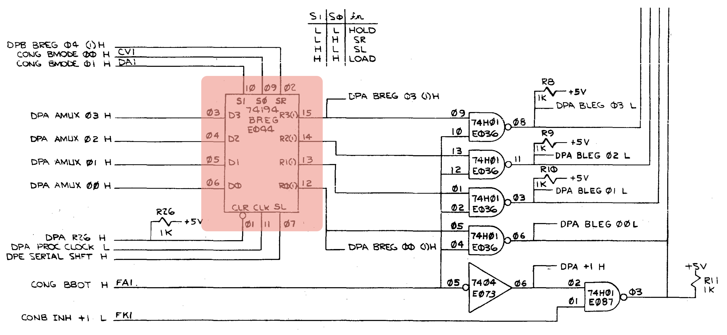
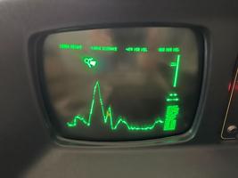
This part was pulled and replaced, and the ROM terminal emulator could then correctly handle LFs! After a few additional red herring to do with loose power connectors and occasional accidental bumping of the test switches on the M7013 display control board, Scott was also able to get the lunar lander code to load and run via the ROM bootstrap binary loader, though still with some display problems:
Scott discovered a major clue concerning remaining loader problems: some GT40 binary-loader encoded binaries we had been using which were downloaded off other enthusiast web sites contained erroneous extra linefeed and "!" characters, which confused the loader and/or triggered bad checksums. After stripping these out, the loader was seen to work quite reliably.
With diagnostics now in hand, Scott was able to track down a few remaining hardware issues on the display boards (a bad register with a stuck high bit, and a swap of one of the DACs which had been acting flaky with one from a spare board. I don't have precise details on these particular fixes, but will expand here later if/when I get more information.)
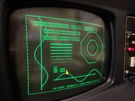
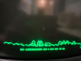
Below, screen shots of some diagnostics, and at long last, Scott lands on the moon and gets his cheeseburger! Drop by and visit Scott at his booth at VCFMW this weekend, see and play game, and hear tales of the restoration first-hand!
GT40 Terminal
Mon 21 August 2023 by Fritz MuellerA while ago my friend Scott approached me with an idea to collaborate on restoration of a DEC GT40 graphic display terminal of unknown status, belonging to a third collector friend of ours; the idea was to restore the machine to working order for exhibition at the various summer/fall vintage computer shows. The GT40 ran an early (pre-Atari) graphical version of the lunar lander game which was released in 1973. The 50th anniversary of this code seemed a nice theme for the exhibit.
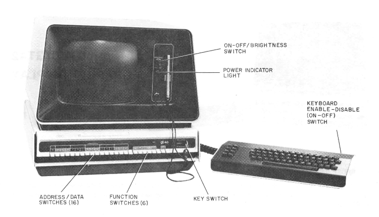
The GT40 was an integrated product consisting of a PDP-11/05 (KD11-B) CPU, a VT11 vector display processor, a VR14 X-Y monitor, a light pen, keyboard, and a DL11 serial interface:
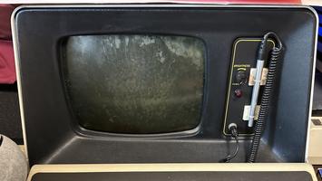
Scott retrieved the terminal, which had a fairly bad case of screen rot. We agreed that Scott would work on restoration of the monitor while I dug in on the system unit. Scott got to work while I dealt with distractions of ongoing home renovations, a ton of work-related travel, and my first bout of COVID (blaargh!)
The screen rot is caused by a deterioriation of a polyvinyl acetate (PVA) layer sandwiched between the front surface of the CRT glass and an outer protective implosion shield. All of this is held together by a retaining ring affixed to the CRT with silicone adhesive. The only fix for this is to disassemble the monitor, separate the sandwich, and clean out and replace the deteriorated PVA layer.
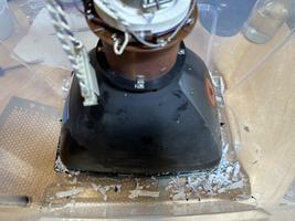
After chatting with some folks who had successfully conducted a similar VR14 restoration at the Rhode Island Computer Museum, Scott obtained some silicone digester to aid in separation of the retaining ring. The terminal was disassembled and then digester was repeatedly injected under the ring with a syringe, allowed to sit, and the resulting softened silicone scraped away over the course of a week.
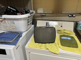
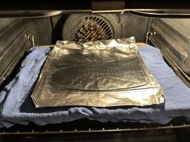
Scott then worked to conform a lexan sheet to the interior of the implosion shield as a replacement for the PVA layer, as RICM had done. This process, conducted in a home oven, proved to be quite fiddly. But persistence paid off, and the end result looks very nice!
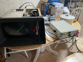
After a precautionary reform of the larger power supply electrolytics, careful reassembly, and a gradual bringup on a variac, the monitor showed proof of life on the bench, hooked up to a signal generator source.
In the meantime, starting to feel better, I began to look at the CPU unit. Power supply electrolytics appeared to be in good shape, and the supply came up on the bench without much difficulty.
The module utilization for this backplane is as follows:
| A | B | C | D | E | F | |
|---|---|---|---|---|---|---|
| 1 | A320 VT40 Display Generator | |||||
| 2 | M7013 VT40 Display Control | |||||
| 3 | M7014 VT40 Bus Control | |||||
| 4 | M7800 DL11 Serial | |||||
| 5 | M930 Term. / UNIBUS out | H214 Core Stack (8K x 16) | ||||
| 6 | G231 Core Memory Driver | |||||
| 7 | G110 Core Memory Control | |||||
| 8 | M7261 KD11-B Control | |||||
| 9 | M7260 KD11-B Data Paths | |||||
On the assumption (later proved wrong) that this was effectively the same as a PDP-11/05 setup, I began debug with just the two CPU cards, an M9301 boot/terminator in position 5A-B, and a grant continuity "knuckle buster" in position 4D. Some problems were immediately apparent from the front console: deposit and examine operations to various memory-mapped CPU registers seemed to work as expected, but when examining contents the M9301 ROM locations bit 13 was always displaying zero. The CPU would not enter run mode, nor could it be single stepped.
Docs suggested that the GT40 would accomodate a KM11 debug module in postion 1B, so in this went. The machine behaved even more strangely when the KM11 was in, hanging up entirely unless the KM11 was put in manual clock mode, and even then stepping microstates at unexpected times. It took a little probing of the CPU clock circuits to discover why:
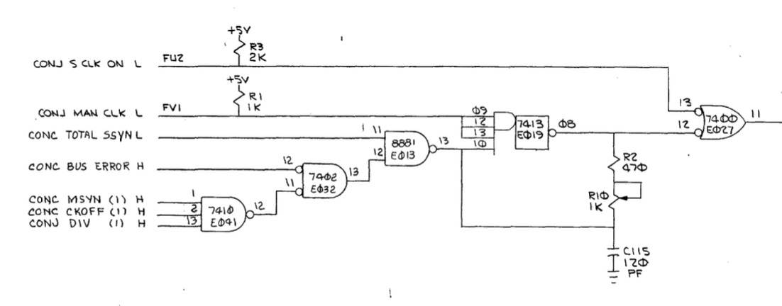
Here we see the RC clock at E019. CONJ MAN CLK L is wired to KM11 switch S2, and inhibits the RC clock when pulled low. With the RC clock thus disabled, NOR gate E027 admits manual clocking via CONJ S CLK ON L, connected to KM11 (momentary) switch S4. The output at E027 pin 11 continues downstream from here as the basis of the main processor clock signal.
As it happened, momentary switch S4 was wired on my KM11 replica with opposite sense from that expected. Thus in its resting postion CONJ S CLK ON L was asserted (low), which meant the clock output at E027 pin 11 was forced constantly high, regardless of the state of the RC clock. This was verified by leaving S2 "off" and pulling S4 over to its momentary position, whence the CPU clock immediately picked up again.
I had never noticed this switch reversal when using the KM11 with the 11/45, the RK11-C, or the 11/34 -- all of these have different clocking circuits unaffected by the default postion of S4. Desoldered and rotated S4 180 degrees, and the problem was fixed.
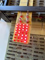
After having addressed this, I single stepped through a few of the console microcode flows and was able to match the microcode listings to what was displayed on the KM11 and the console lights with some success. An action shot of the KM11:
A few tips for anybody else who might be micro-stepping the KD11-B CPU, while we are here:
-
The MPC address displayed on the KM11 is negated -- dark LEDs are ones, and lit LEDs are zeros. This definitely takes a little getting used to...
-
The MPC address displayed on the KM11 is the address of the next micro-instruction, not the current one. This is also pretty tricky until you get the hang of it. One nice thing about it, though, is that the displayed next address does include the wired-or outputs of micro-branches.
-
Each manual clock toggle is one bus clock, and typically, a micro-instruction will take two bus clocks to execute. An exception is the inner part (single shifts) of the micro-flows for shift and rotate instructions, which only take a single bus clock. Generally, it is useful to go ahead and advance two bus clocks at a time, as it is easy to get confused probing for signals that by design aren't clocked until the second bus clock within the micro-instruction.
-
The console lights are hard-wired to always display the ALU B-leg input. Useful intermediate information is often displayed there intentionally by the microcode flows.
Now it was possible to put the data paths board out on extenders and step the microcode for a console examine of a ROM location with bit 13 set, and see why bit 13 never showed up on the console lights. To understand this properly, we need to see an excerpt of the KD11-B data paths:
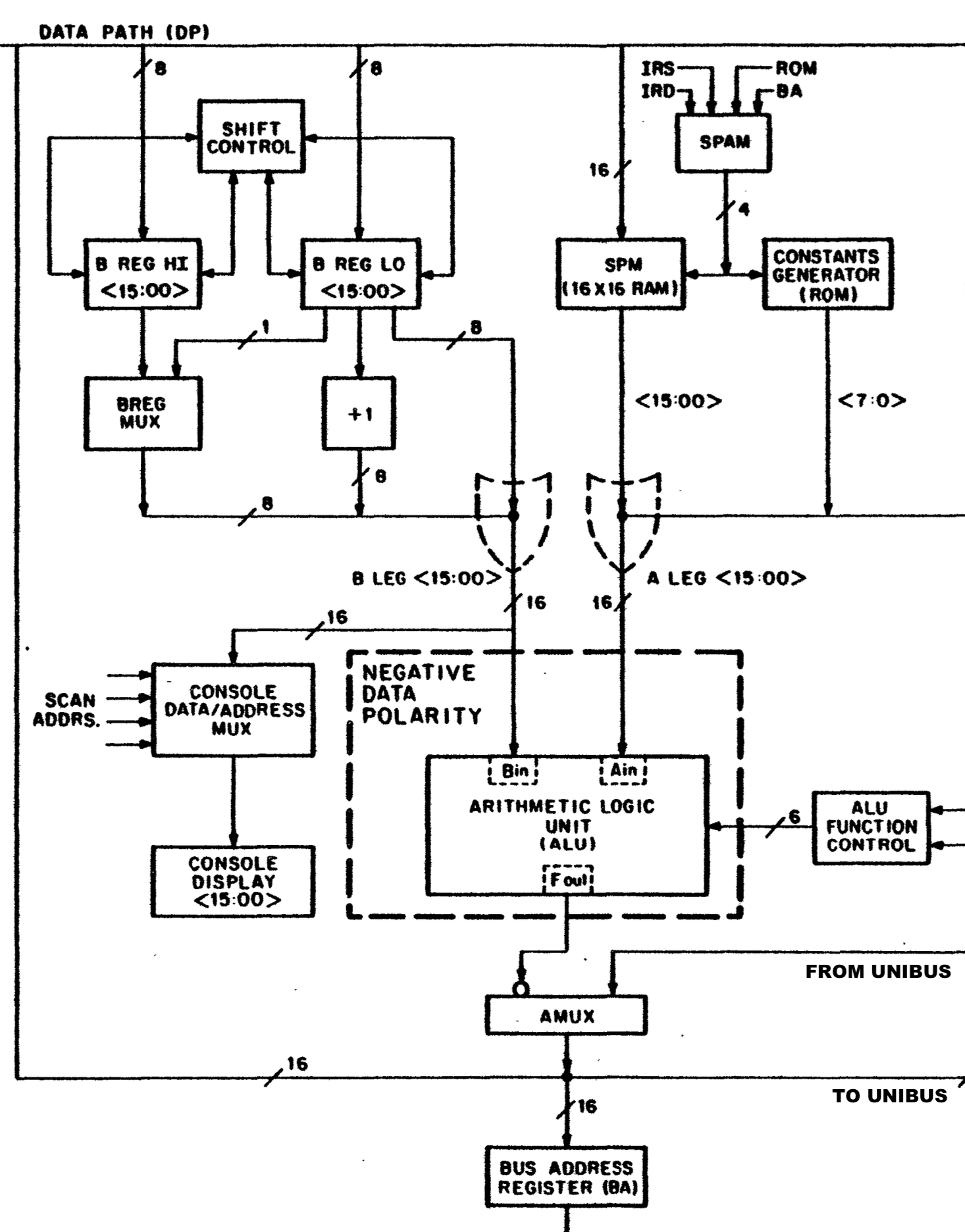
Here you see the ALU in the middle, fed by its B-leg and A-leg inputs. B-leg is fed from the B-register, with provisions for shifting, sign-extension, or forcing the constant +1. B-leg is also continuously displayed on the console lights. A-leg contains, significantly, the 16-location scratch-pad memory (SPM). The first eight locations of this hold processor registers R0 through R7; the remaining eight locations serve as temporary registers for use by the microcode. A-leg can also provide misceallaneous constants from a small ROM.
The A-mux, below the ALU, determines whether the main processor data path is fed from the ALU output, or from the UNIBUS data lines.
With this in mind, the relevant microcode source sequence (taken from the listings in the engineering drawings) is as follows:
LOC  NXT  * CONSOLE EXAMINE SWITCH- FIRST TIME IN SEQUENCE (DON'T INC R[17])
          / GET TO CE1-1 FROM H-2 VIA BUT SWITCH
          / GET TO CE1-1 FROM CE2-2 VIA GOTO
317  307  CE1-1 BA,B←R[17]; BUT SWITCH
          / DISPLAY ADDRESS BY PUTTING INTO THE B REGISTER WHILE EXAMINE IS DOWN
          / LOOP ON CE1-1 UNTIL SWITCH IS RELEASED
307  326  CE1-2 DATI; CKOFF
326  302  CE1-3 B←UNIBUS DATA; GOTO H-2
At micro-location 317 (state CE-1, "console examine 1"), the bus address register and B-register are loaded from SPM location 17, which holds the current console load/examine address. BUT SWITCH ("branch micro-test switch") causes the microcode to loop here as long as the examine switch is depressed. During this time, the fetch address is displayed on the console lights since it has been loaded into the B-register. This was all observed to be functioning normally.
When the examine switch is released, we branch to micro-location 307. Here, a UNIBUS read (DATI) bus cycle is initiated, and the processor clock and microcode execution are suspended until the bus target asyncrohonously asserts SSYN (indicating valid data on the bus) or alternatively times out. The bus cycle was observed to occur normally, leaving SSYN and the correct data (including a correct bit 13) asserted on the UNIBUS.
Proceeding to micro-location 326, we see that the A-mux should be set up there to admit the data from the UNIBUS to the main processor data path and then the B-register should be latched for display. Here a problem was apparent. Sheet DPD of the GT40 engineering drawings covers bits 15:12 of the data paths; package E015 there is an 8266 2x4 mux which implements that slice of the A-mux. E015 was seen via logic probe to be set up with correct select codes and correct input from the UNIBUS. UNIBUS bit 13 was not being correctly passed on to its corresponding output, however -- a failed part.
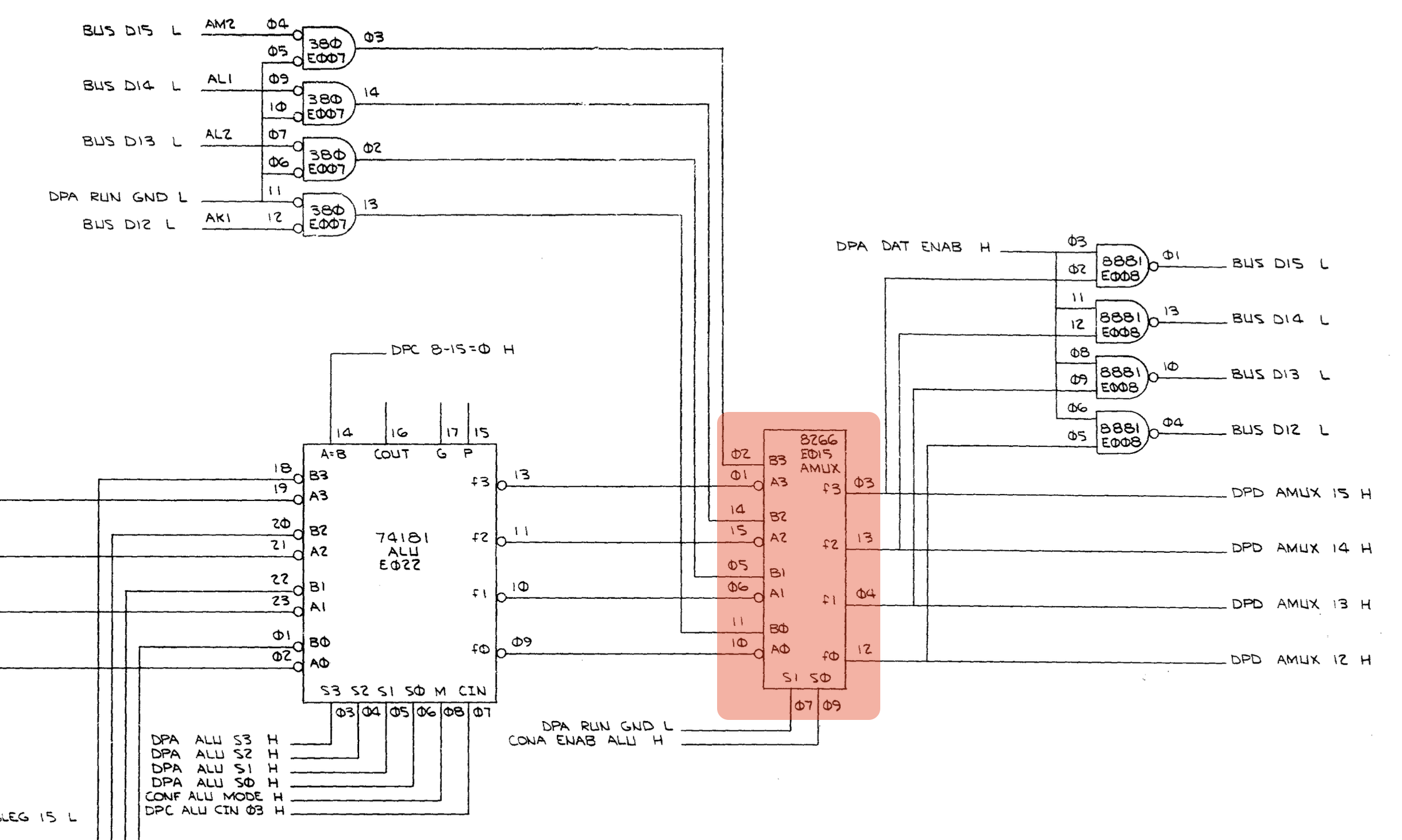
The 8266 is out of production and somewhat rare; for the time being a functioning 8266 was "borrowed" from a spare GT40 data paths board that we obtained from our fellow collector. Removed the bad part, socketed, and replaced with the borrowed part, and the bit 13 display problem was fixed!
Moving next to the run/step problem, the machine was seen to be hanging up in micro-state F-3, after initiating the DATI bus cycle to fetch an instruction. This lead to investigation of some of the the bus control logic, as detailed on sheet CONC of the engineering drawings:

The CPU must negotiate for control of the UNIBUS and assert BBSY if successful. Here I could see the DATI request being successfully latched, but BBSY assertion was blocked at E014 by CONC NPR GRANT H, a non-processor request (DMA) bus grant. Sure enough, some more probing indicated the the processor had issued a NPR grant because it was reading an NPR request over the UNIBUS. Where was that coming from with nothing else in the system?
Well, it turns out in the GT40 the near-side bus termination is integrated onto the M7014 GT40 bus control board that must but in slot 3, so you can't really debug without this card in place! (It could be that an additional M930 terminator in 3-A,B would work, as in a stock 11/05, but I haven't checked the backplane wire list in detail to be certain of this.) In any case, slotted in the M7014, and the machine began to behave much more rationally with a properply configured bus...
Went for broke and slotted in the rest of the display interface boards and (why not?) the core memory and DL11 as well. The machine was showing very promising signs of life. The terminal emulator in the bootstrap ROM ran and was able to render recevied characters on the display! Characters typed on the keyboard were also successfully forwarded out the DL11. A line feed character typed to the terminal emulator seemed to crash it, so that still needed to be looked into. Took the time to toggle in a small test program from the user guide, and this executed correctly rendering a square on the display, indicating most of the logic in the display interface boards was also functioning correctly:
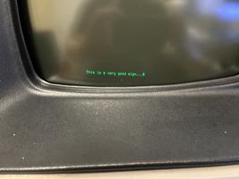
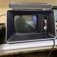
The toggle-in program running above:
1 2 3 4 5 6 7 8 9 10 11 12 13 | 000100 012706 000500 START: MOV #500,R6 ; SETUP STACK
000104 012737 002000 172000 MOV #TABLE,@#DPC ; START VT11 ON TABLE
000112 000001 DONE: WAIT ; LET NPR HAPPEN
000114 000776 BR DONE ; KEEP WAITING IF INTERRUPTED
002000 117124 TABLE: .WORD POINT+INT4+LPOFF+BLKOFF+LINE0
002002 000500 000500 .WORD 500, 500
002006 110000 .WORD LONGV
002010 040200 000000 .WORD 200+INTX, 0
002014 040000 000200 .WORD 0+INTX, 200
002020 060200 000000 .WORD 200+INTX+MINUS, 0
002024 040000 020200 .WORD 0+INTX, 200+MINUS
002030 160000 002000 .WORD DJMP, TABLE
|
Tried to get some program uploads going over the built-in binary loader in the bootstrap terminal emulator, but this didn't seem to be quite working, either. Took a short break for dinner, returned to examine this further, ran for a few minutes, then disaster... Something in the CPU let go, and the machine was once again unable to execute code.
Digging in on this new failure a little, when attempting to single step ROM code from the front panel, the PC was seen to increment by +1 instead of the expected +2; this resulted in an immediate bus error that halted the machine. Back in goes the KM11, then, and the same microcode stepping technique was used to begin investigating.
So how does the KD11-B (ostensibly) increment the PC by 2? It turns out this is done by selecting the PC (SPM location 7) onto the ALU A-leg, constant +1 on the ALU B-leg, and introducing the additional +1 at the carry input of the least significant bit slice of the ALU on sheet DPA of the engineering diagrams:
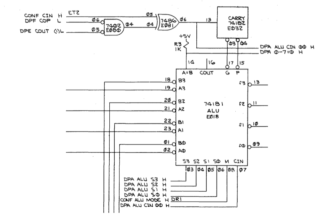
Signal CONF CIN H comes from microcode, wire-or'd with output of operation decode ROMs in the ALU aux control circuitry. In this case, the logic probe revealed that this signal was erroneously low; further investigation revealed that microcode PROM CONF E094 had failed:
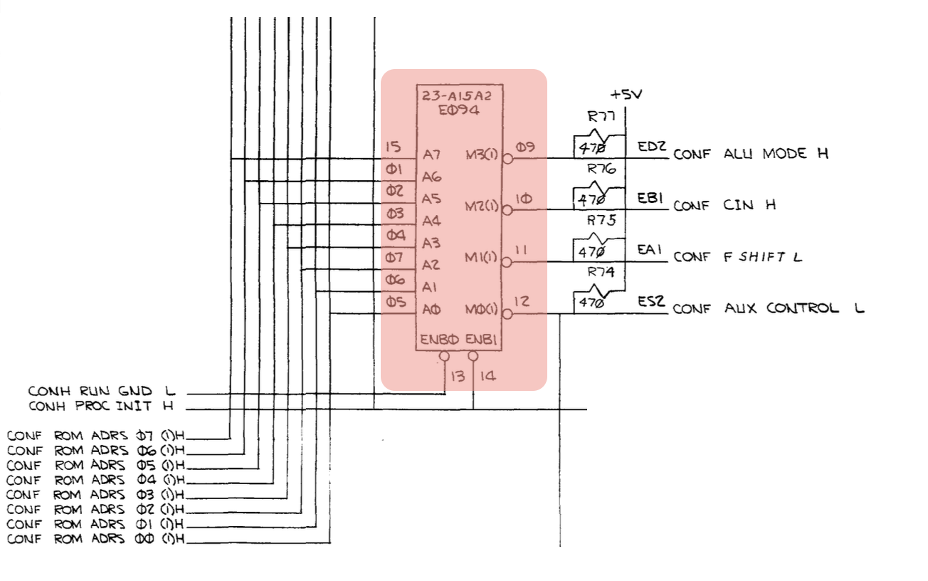
Alright, this is an IM5603 (equiv. 82S126N) bipolar PROM, and I don't happen to have that in stock. So now we're stuck until we can source one. At this point, the day job once again intervened, and I needed to prepare to head off to the Rubin Observatory in Chile for a couple of weeks. Scott came by to pick up the work in progress; had time to share a short demonstration of microcode debug techniques, then off to pack and prepare for my trip...
[ to be continued... ]
Apple II Plus: power supply and language card
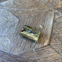
Mon 21 March 2022 by Fritz MuellerOkay, so the Apple II Plus I was using to test the VM4209 monitor worked fine for about a half hour, then smoked a RIFA cap in its power supply. These are a very common known failure in various old microcomputer power supplies, and I really should have already caught this on inspection and shotgunned it. Boy, do they generate a lot of smoke and stink when they go...
Electrolytics in here are also all pushing 40 years at this point and Astec opted for only 85C parts for many of these, so I went ahead and ordered a whole replacement kit from Console5. I replaced the front end filters and anything on the back end that was 85C or looked even slightly bulgy, which ended up being most of them:
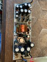
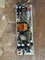
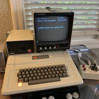
Put it all back together and back in business, except noticed an additional problem: DOS 3.3 booted but neither recognized nor loaded the "language card" (soft ROM) present in the machine. Since my machine has Applesoft BASIC in system ROM, this meant no Integer BASIC (and no ROM mini-assembler) for me until this was fixed.
For those who might not be familiar with the Apple II language card, it provides several features. An Apple II or II Plus can have at most 48K of RAM on the system board. The overall memory map looks like this:
| $0000-$BFFF | RAM (48K) |
| $C000-$CFFF | IO space (4K) |
| $D000-$FFFF | ROM (12K) |
The first thing the language card provides is a 2K ROM which by default overlays whatever ROM is in the system
board socket for addresses $F800 to $FFFF. This ROM holds the 6502 reset vector and the boot monitor; the
version provided on the language card has an "autostart" capability that will search for and boot off an
attached Disk II floppy. I am not sure why Apple provided this ROM on the language card since the same ROM
could be upgraded directly on the fully-socketed system board, and indeed everything after the Apple II Plus
came with this autostart ROM pre-installed. Possibly this was done for maximum backward compatibility with
Apple's previously-offered "Firmware Card", which also contained this ROM? Third-parties would later offer
clones of the language card that did not contain the additional/redundant F8 ROM, and nobody seems to have
particularly cared or noticed...
The second thing the language card provides is an additional 16K of RAM. This can be loaded, then
write-protected and mapped over the entire ROM space of the machine from $D000 to $FFFF, providing a "soft
ROM" capability. Since the available ROM address space is only 12K, the leftover 4K or RAM on the language
card is bank switchable at address range $D000 to $DFFF.
Advanced software which doesn't depend on the system ROMs at all can also map the RAM over the system ROM
address space and leave it in read/write mode, thus gaining access to a full 64K of RAM (with the caveat of
the switched bank at $D000.)
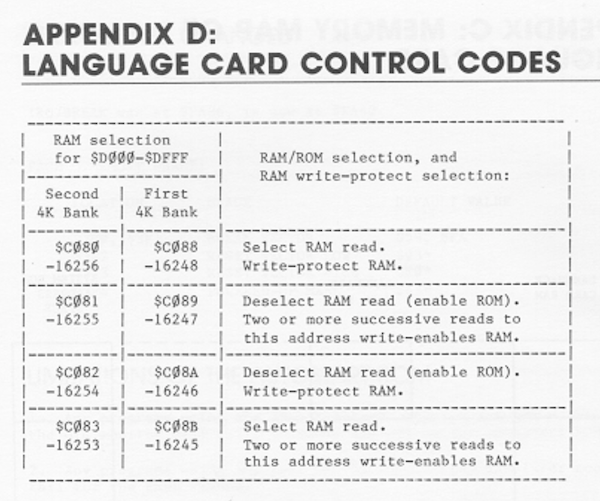
The language card programming interface presents as follows:
My goal is to be able to run the initial (1980) release of Apple DOS 3.3. This version loads up the language card at boot in soft ROM mode with Integer BASIC and an older version of the F8 monitor ROM, which contains a few extra niceties like a built in mini-assembler and primitive step/trace capabilities. A system so loaded can then be conveniently switched back and forth between BASIC and monitor versions with the DOS "INT" and "FP" commands. But detection of my language card seemed to be failing, so it was never loaded up at boot. Attempts to manually load and activate it also came to naught.
So, time to dig in and see what's going wrong... DOS 3.3 does initial checks and setup of the language card
via a small machine language program, loaded into RAM at boot by the DOS master disk's HELLO BASIC program.
Machine code is used for this part rather than BASIC so the probe/setup code can be placed and run from RAM
outside the mapping range of the language card (the BASIC interpreter itself running from ROM addresses
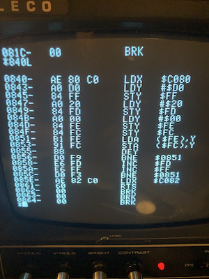
within this mapping range). Here is the machine language program, after being POKEd into RAM by HELLO,
listed via the ROM monitor:
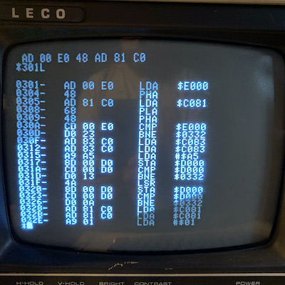
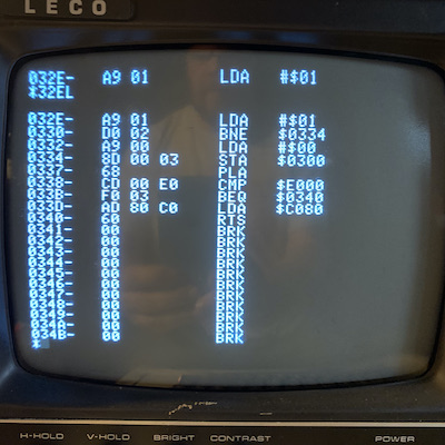
I interpret the actions of this code as follows:
-
The code first retrieves and stashes the contents of location
$E000, within the mappable address range. A read of$C081then maps the ROMs on the system board (see programming interface above), and the contents of$E000are checked again. If the contents now differ, the code assumes the card, now in mapped ROM mode, was previously in mapped RAM mode, and it jumps to address$0332to put things back the way it found them and bail out. -
If not, the code reads from address
$C083twice, which puts the card, if present, in writable mapped RAM mode. Two different values are written to and compared back from location$D000. If a language card is not present, this location will still be mapped to ROM on the system board, and at least one of these compares will fail; if either one does, the code jumps to$0332to bail out. -
Otherwise, we've verified that a card is present and wasn't already in active play. The program now reads from address
$C081twice to move back to mapped ROM mode, but leaving RAM writable to be loaded by the remainder of theHELLOprogram after return (in this mode, reads will come from system ROMs, but writes will go to the corresponding locations in language card RAM). A success return code is loaded, and the code jumps forward to the exit code at$0334to return to the caller. -
The bail out routine at
$0332just sets up a fail return code, then falls through to$0334. Code here stores the return code to the return code location and does one last compare between the stashed and current values at$E000to determine if mapped RAM mode must be restored; if so this is done via a read from location$C080(RAM is left write-protected). Control is then returned to BASIC.
In any case, the above is what the code does, even if I may have misinterpreted some of its motivations. On
my system, the ROM on the language card seemed to be working correctly (monitor ran fine, but if ROM on
language card was pulled the machine failed to boot, indicating the monitor was in fact running successfully
out of ROM on the card). However, mapped RAM mode seemed never to engage. The machine code snippet above
returned "00" without crashing, and the DOS HELLO program assumed no card present. Manually accessing the
appropriate control registers also had no effect.
The language card design does not seem to be documented in detail, but a schematic is available and it is not too hard to suss out. The first thing to check would seem to be the register interface. Here is an excerpt from the schematic, with a couple of annotations added:
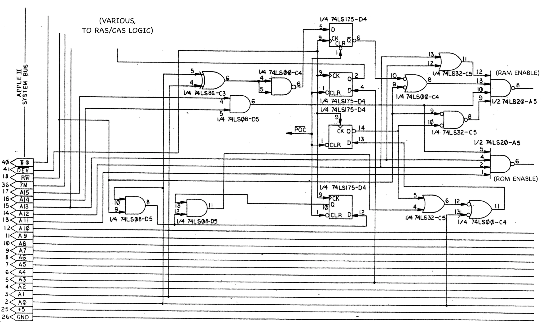
The register interface is principally implemented by a 74LS175 quad flip-flop at D4. These flip-flops share a common reset at power-on, and a common clock based on the expansion slot DEV_L signal; DEV_L is a slot-specific signal strobed by the system on any bus cycles to IO address space allocated to that slot. Examination of the programming interface along with address line decodes feeding the D inputs here leads to the conclusion that the top-most flip-flop holds RAM/ROM mapping mode, the next one down is RAM bank select, the next is RAM write-enable, and the last is a one-bit count to support write-enable after only two successive reads.
Put a chipclip on at D4, and observed behavior of the flip-flops on the logic analyzer while exercising the control registers via the monitor. Problems were apparent right away: while the bank select and count flip-flops were responding as expected, the mapping mode and wite-enable flip-flops were not. The shared reset and clock appeared correct, and all flip-flops themselves were responding logically correctly with respect to their inputs. The issue was apparently with the incoming D lines to two of the flip-flops. Starting with the ROM/RAM enable flip-flop, then, that D line is fed via C3 and C4. And a visual inspection in preparation for clipping these up for the analyzer revealed that, surprisingly, these two chips had actually been reversed on the board!
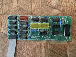
The language card is fully socketed, so presumeably this reversal had occured during previous troubleshooting or service by the former owner? In any case, it was easy to swap the chips back to their correct locations, and the logic analyzer showed that the entire register interface seemed to be behaving according to design after that. DOS 3.3 now recognized the card at boot (yay!), but the system would crash after loading and mapping the RAM. So, maybe a bad RAM chip as well?
To troubleshoot the RAM, I followed a technique described in this video on the "Adrian's Digital Basement" YouTube channel. Basically, a couple short machine language programs, entered and executed via the monitor, to copy ROM contents into the language card RAM, then copy back out to another location in system RAM. This allows a comparison of source data in ROM and round-tripped data in system RAM; a mismatch indicates a RAM problem on the card. Here are the two programs I used and, and dumps of the resulting data:
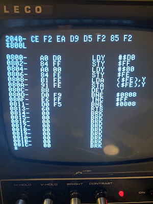
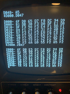
And sure enough, it's quite visible here that bit 7 is having problems. Swapped out the 4116 at A2, and that seems to have done it for this one. Now I need to go find a copy of Choplifter...
Sanyo VM4209
Sun 13 March 2022 by Fritz MuellerSome time back I purchased a Sanyo VM4209 B&W video monitor on eBay. Sold as working, it arrived with apparently working horizontal but no vertical deflection. The price had been right, however, so it was just shelved into the repair queue.
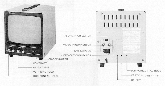
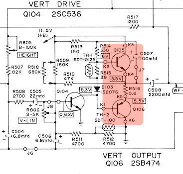
I now have a few DEC VT series terminals to work on and would like to have a small video monitor available on the bench for this, so I pulled down the VM4209 to give it a look. Given the lack of vertical deflection, the first thing to check would be the vertical deflection power transistors, Q105 and Q106 here:
It turns out these transistors are quite well buried in the guts of the monitor on a small aluminum heat sink. Took a while to work my way in to them, and required unsoldering a few leads and removing the CRT:
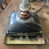
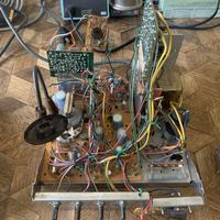
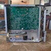
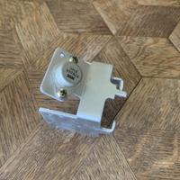
Sure enough, the lead connecting Q106 collector to ground had been broken, and the part tested bad. Q105 appeared healthy, and there were no other apparent signs of distress in the surrounding circuitry. Q106 is an out of production 2SB474 germanium PNP in the less common TO66 package; I opted to replace it with the "modern" equivalent NTE226. Re-assembled, and was greeted immediately with a functioning raster. Pulled out an Apple II Plus to test with:
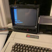
This was quite fun for a short while, until a RIFA cap in the Apple II power supply let go, filling the dining room with acrid smoke. So, expect an additional article on that one in the near future :-)
BASIC-11 under RT11
Sun 15 August 2021 by Fritz MuellerI figured it might be fun to play around a little bit with BASIC-11 under RT11 on the newly-restored PDP-11/34. If I got that working, it could also be included on the RK05 RT11 disk image that I use regularly for demos on the larger PDP-11/45.
The first thing to do was to find a compatible disk image and get it running under simh. Bitsavers had
BASIC-11_V2.1_RX02.DSK.zip, which would seem to fit the bill, but the contained image would not mount
successfully on simh's RY device. Looking through a dump of the image, there was an apparent "RT11A"
signature, so that looked promising. Tried putr under dosbox as well, but it would hang mounting the image.
So, off to the cctalk mailing list for some advice...
Glen Slick on the list first noticed a file size discrepancy:
That BASIC.DSK image file has a size of 486,400 bytes. I don't know where that size would come from.
A physical RX-02 floppy should have a sector size of 256 bytes, with 26 sectors per track, and 77 tracks, which would be a total of 512,512 bytes, or 505,856 bytes if the first physical track is ignored.
Indeed, the other RX-02 floppy images available here do have a size of 505,856 bytes: http://www.bitsavers.org/bits/DEC/pdp11/floppyimages/rx02/
Hmm, maybe that BASIC.DSK image file was created by something that only copied the initial allocated logical sectors and ignored unused logical sectors at the end of the floppy, and maybe PUTR doesn't handle disk image files that are not the expected full size?
Example of padding the 486,400 byte BASIC.DSK image file to a size of 512,512 bytes on a Windows system:
FSUTIL FILE CREATENEW BLANK 26112
COPY /B BASIC.DSK+BLANK TEST.DSK

C:\PUTR>DIR TEST.DSK
Volume in drive C has no label.
Volume Serial Number is 14CE-1A29
Directory of C:\PUTR
08/11/2021  12:55p             512,512 TEST.DSK

C:\PUTR>PUTR
PUTR V2.01  Copyright (C) 1995-2001 by John Wilson <wilson@dbit.com>.
All rights reserved.  See www.dbit.com for other DEC-related software.

COPY mode is ASCII, SET COPY BINARY to change
(C:\PUTR)>MOUNT RX: TEST.DSK /RX02 /RT11 /RONLY
(C:\PUTR)>DIR RX:

Volume in drive RX is RT11A
Directory of RX:\*.*

11-Aug-2021
BSOT0D.EAE    12  04-Apr-1983
BSOT0S.EAE    10  04-Apr-1983
BSOT1D.EAE     9  04-Apr-1983
BSOT1S.EAE     6  04-Apr-1983
BSOT0D.EIS    12  04-Apr-1983
...
...etc. Nice. Still no luck mounting under simh, though. Glen further offers:
As far as I can tell by default PUTR expects to work with logical sector order RX-02 disk images that are 512,512 bytes in size. The BASIC-11 RX-02 disk image available here is in logical sector order, but is less than 512,512 bytes in size: http://www.bitsavers.org/bits/DEC/pdp11/floppyimages/rx02/ PUTR appears to be unhappy with the disk image unless it is padded to 512,512 bytes in size.
On the other hand as far as I can tell by default SIMH expects to work with physical sector order RX-02 disk images. If I mount the logical sector order RX-02 disk image that works with PUTR in SIMH, then RT-11 gives a "?DIR-F-Invalid directory" error. If I translate the logical sector order RX-02 disk image back into a physical sector order disk image (dealing with track shifting, sector interleaving, and track to track sector skewing) then RT-11 on SIMH is happy with the disk image.
and:
One bit of information that I found helpful as a reference when I looked at this quite a while ago was the 2.11BSD RX02 floppy disk device driver source code, which can be viewed online here:
https://minnie.tuhs.org/cgi-bin/utree.pl?file=2.11BSD/sys/pdpuba/rx.c
In particular, the routine rxfactr(), which as the comment says it calculates the physical sector and physical track on the disk for a given logical sector.
I used that as a starting point to write a simple utility to read an RX-02 disk image file in logical sector order and output an RX-02 disk image file in physical sector order.
/*
*  rxfactr -- calculates the physical sector and physical
*  track on the disk for a given logical sector.
*  call:
*      rxfactr(logical_sector,&p_sector,&p_track);
*  the logical sector number (0 - 2001) is converted
*  to a physical sector number (1 - 26) and a physical
*  track number (0 - 76).
*  the logical sectors specify physical sectors that
*  are interleaved with a factor of 2. thus the sectors
*  are read in the following order for increasing
*  logical sector numbers (1,3, ... 23,25,2,4, ... 24,26)
*  There is also a 6 sector slew between tracks.
*  Logical sectors start at track 1, sector 1; go to
*  track 76 and then to track 0.  Thus, for example, unix block number
*  498 starts at track 0, sector 25 and runs thru track 0, sector 2
*  (or 6 depending on density).
*/
static
rxfactr(sectr, psectr, ptrck)
   register int sectr;
   int *psectr, *ptrck;
{
   register int p1, p2;

   p1 = sectr / 26;
   p2 = sectr % 26;
   /* 2 to 1 interleave */
   p2 = (2 * p2 + (p2 >= 13 ?  1 : 0)) % 26;
   /* 6 sector per track slew */
   *psectr = 1 + (p2 + 6 * p1) % 26;
   if (++p1 >= 77)
       p1 = 0;
   *ptrck = p1;
}
An RX02 image shuffled into physical sector order generated by Glen and suitable for use with simh is attached here.
Jerry Weiss further suggested that the original, logically ordered image may work as is under simh if attached as an MSCP device rather than RX02. This turns out also to be the case:
On Fri, Aug 13, 2021 at 9:46 AM Jerry Weiss wrote:
Could you attach logical sector (block?) image as MSCP disk in SIMH? Other than some minor image manipulation for removing track 0 if present, is there any reason this would not be readable?Hmm, it didn't occur to me to try that. Mounting the logical sector order RX-02 disk image, without any modification necessary, as a raw MSCP disk does indeed appear to work!
sim> ATTACH RQ1 BASIC.DSK
RQ1: 'BASIC.DSK' Contains RT11 partitions
1 valid partition, Type: V05, Sectors On Disk: 950

sim> SHOW RQ1
RQ1     486KB, attached to BASIC.DSK, write locked
       RD54, UNIT=1, autosize
       RAW format

.DIR DU1:

BSOT0D.EAE    12  04-Apr-83      BSOT0S.EAE    10  04-Apr-83
BSOT1D.EAE     9  04-Apr-83      BSOT1S.EAE     6  04-Apr-83
BSOT0D.EIS    12  04-Apr-83      BSOT0S.EIS     9  04-Apr-83
BSOT1D.EIS     9  04-Apr-83      BSOT1S.EIS     6  04-Apr-83
BSOT0S.FIS     7  04-Apr-83      BSOT1S.FIS     6  04-Apr-83
...
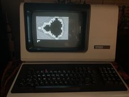
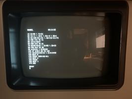
...etc. Armed with the above, I was able to get BASIC-11 into an RT11 image in the Unibone card, and running on the new PDP-11/34. Here's output from the DEC BASIC mandelbrot program at rosetta code:
Unibone
Wed 24 March 2021 by Fritz MuellerI have been keeping an eye on Jörg Hoppe's interesting Unibone project for some time -- it is a general-purpose Unibus device emulator and diagnostic tool, built around a BeagleBone Black compute module running embedded real-time Linux. The PDP-11/34 restoration project finally provided enough impetus for me to pull the trigger on getting one.
Sent Jörg an email to order a kit, which arrived some weeks later complete with bundled BeagleBone. The kit is pretty well thought-out and was enjoyable to put together. Had to throw in a few of my own pin headers and jumpers to complete the assembly. The only other small confusions were a few of the resistor packs which did not match the schematic (Jörg informed me these are non-critical values.)
The kit did not include card handles. I decided to try having some 3D printed by Shapeways, using their "processed versatile plastic" process, which is a laser sintered nylon, color dyed and smoothed. I used a card handle model by Vince Slyngstad found here. The results were nice, sturdy, and dimensionally correct. The chosen "purple" color is a rather intense magenta in real life. Not exactly cheap for just a couple parts, but I had been wanting to try their print service.
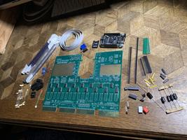
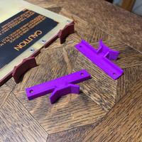
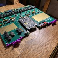
The Unibone has all sorts of capabilities, and proved itself very useful during the '11/34 restoration:
-
Ability to bus master to probe the Unibus address space and run diagnostics on memory found there. This was very useful for debugging the memory card that came with the -11/34 and sussing out its undocumented configuration switch settings.
-
Ability to directly load and execute MAINDEC diagnostics, without needing a functioning console emulator or storage subsystem. This is a convenient and speedier alternative to PDP11GUI.
-
Subsequently, the ability to emulate entire storage subsystems, very useful for loading and running full operating systems on this -11/34 which otherwise has no storage of its own.
The Unibone goes in a quad SPC slot; I opted for slot 9 on the -11/34, and this entailed removing the NPG jumper on the backplane there to allow the Unibone to bus master. The device worked well straight-away after assembly.
There are, alas, a couple small frustrations with the current design:
-
It is desireable to configure the Unibone and backplane to allow the Unibone to bus master and interrupt. However, this leaves grant chain(s) open at boot until the Unibone's own embedded software can boot and take control of the card (which takes on the order of a minute or so). During this time the host system is non-functional or may hang, and it needs to be subsequently reset (this reset can be scripted from the Unibone, but all of this does significantly increase end-to-end boot time of the machine). It would be nice if the Unibone had something like some normally-closed relays on the grant chains, to preserve grant continuity until control is actively assumed.
-
It would be desireable to be able to power the embedded BeagleBone in isolation, in place in a system, without having to having to have the entire host system powered at the same time (e.g. for maintenance of the Unibone's embedded software stack, maintenance of locally stored storage system media images, etc.) There is a relay on the Unibone which switches in Unibus power when available, but unfortunately, the design is such that if the BeagleBone is also externally powered the relay remains engaged when the host system is shut down. This could lead to the BeagleBone trying to power then entire Unibus via its 5V supply/connector, which could obviously be problematic... For now it seems best just to pull the card in order to run it in isolation, which is a little less than convenient.
That said, the designs and software are open source, and the card comes with some generous prototyping areas built right in, so some mods to address these issues could be a fun project. All in all, Jörg has put together a fantasically useful bit of kit, and I'm certainly glad to have it in my toolbox!
PDP-11/34
Tue 09 March 2021 by Fritz MuellerThis spring I worked on repair/restoration of a friend's PDP-11/34. The system was in fairly good shape, but missing a few bits and pieces and with the usual sorts of issues for 45-year-old kit. Started per usual with disassembly, cleaning, and inspection. The BA11-K chassis was in pretty decent shape; just a few scratches requiring some sanding and a little touch-up paint to inhibit future corrosion.
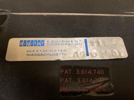
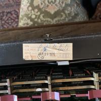
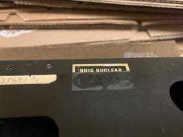
Date codes on the chassis and CPU cards are from 1976, but other components in the chassis are a bit of mix-and-match (a KY11-LB console interface and a third-party Monolithic systems memory board date from 1981, and a DL11-W SLU/RTC card is from 1977). Serial number is 2001. There is also a sticker for "OHIO NUCLEAR", which was an early manufacturer of CT devices.
Foam problems here were limited to a decayed air pre-filter at the front of the chassis and some padding on the cable retaining bar at the rear. A heat gun and a paint scraper are your friend for removing the leftover cellophane adhesive strips that were used to secure the foam. For the replacement pre-filter, I opted for 3M Filtrete carbon pre-filter sheet (part FAPF-UCTF2PAMZ) which comes in sheets large enough to cover the front of the chassis and is easily cut to size with scissors.
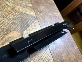
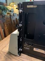
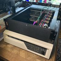
The front panel brackets ended up being a bit of a puzzle to reassemble -- I unfortunately failed to pay close attention to how exactly the lower fasteners were configured during disassembly. Most of the wisdom out in the restoration community seems to pertain to a newer, and much more convenient, version of these brackets (or the ones that arrived on this system were mismatched?) Here's a picture of the brackets that I have, and a shot of the arrangement I finally opted for for the flange-blinded mounting hole at the bottom of the chassis: machine screws driven from the back of the bracket with Keps nuts toward the front. I also added some 1/8" nylon spacers so the pre-filter could be extended across the entire front of the chassis, behind the brackets, and everything still remains square when tightened up. A serviceable replacement power knob was tracked down here.
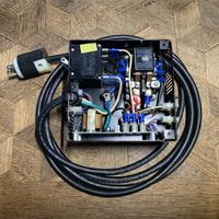
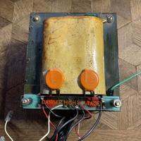
The BA11-K chassis has an integrated H765 power supply. The power-controller unit was in pretty good shape, but I replaced the line cord since the old one had some fairly serious nicks in its outer jacket. Also replaced cap C1 (50uF) which seemed to be drifting off value. Replaced the .1uF across-the-line caps mounted on the power transformer with modern X2 safety caps. The DC regulator modules (2x H744 +5V and 1x H745 -15V) were disassembled and cleaned. Reformed all the large electrolytics, then load tested the reassembled regulators individually. Nothing out of sorts here except the usual replacement of burnt out incandescent indicator bulbs.
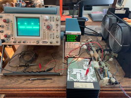
I filled out the system with a near-side M9301 bootstrap-terminator (recent eBay purchase), some G727 "knuckle buster" grant continuity cards, and an M9302 SACK turnaround far-side terminator. New on this restoration was a UniBone Linux-to-Unibus bridge, used to emulate storage devices among other things (more on this in a separate article soon). Checked/adjusted NPR continuity on the backplane (continuity wire wraps in place for all slots except slot 9, to accommodate the UniBone). Module utilization as follows:
| A | B | C | D | E | F | |
|---|---|---|---|---|---|---|
| 1 | M7266 CPU control | |||||
| 2 | M7265 CPU data path | |||||
| 3 | M9301 boot term | M7859 console | ||||
| 4 | Monolithic Systems 303-0158 64 KiB memory | |||||
| 5 | M7856 serial / line clock | |||||
| 6 | G727 | |||||
| 7 | G727 | |||||
| 8 | G727 | |||||
| 9 | M9302 SACK term | UniBone | ||||
Connected up a VT100 to the serial card, and fired things up. Good signs of life from the front panel, but the machine immediately halted without producing a boot monitor prompt. Was able to reset the machine from the front panel, though, and then examine and deposit various memory locations from there.
Boot ROM memory locations were readable, and the contents looked correct. RAM addresses were generally readable and writable, but bit 10 appeared incorrect (sometimes always set; sometimes always clear). I was also able to successfully write to the console XBUF register from the front panel and see characters appear on the VT100.
A bus init from the front panel followed by manually punching in the boot ROM entry point produced a functional ROM monitor on the VT100. Deposits and examines to RAM done from the boot monitor produced results identical to those seen using the front panel (same bit 10 problem).
One of the cool features of the KY11-LB console is a maintenance mode that can run Unibus bus cycles on its own without a CPU. This gives a way to do limited testing of cards in isolation: just set up the M7859 on a powered, terminated backplane segment and plug in cards to be tested one at a time. Deposits and examines can then be done using the buttons and display on the front panel.
Interestingly, when running this way with just the console and memory cards in place the bit 10 errors were no longer apparent. Some other card was apparently corrupting bit 10 on the bus; by checking one at a time the problem was quickly isolated to the M9301 boot terminator card.
The M9301 drives the implicated bit onto the Unibus via an 8881 bus driver at position E9, as seen below. The signal coming in from the bottom here is ENAB DATA H, which is meant to enable these drivers only when the M9301 detects a valid address decode. Verified that data was being incorrectly driven on BUS D10 L at E9 pin 13, regardless of the state of pin 12, indicating a faulty driver. Pulled this, socketed, and replaced (with a compatible ECG 7439), and the bit 10 problem was fixed.
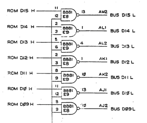
There was still some problem with auto-boot to the M9301 monitor, however; the monitor prompt would now begin to print at power up, but the machine would halt a few characters in. The front panel bus init plus manual jump to monitor entry point workaround was still working though, so put off further investigation of this issue until later.
At this point, given the workaround, the system was working well enough to begin loading and running MAINDEC diagnostics over the serial line with PDP11GUI. Relevant diagnostics, from the PDP-11/34 System User's Manual:
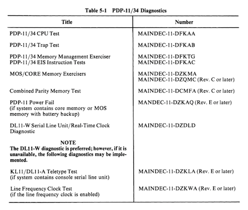
DFKAA, DFKAB, and DKFAC all ran without issue. DFKTG, DZKMA, and DZQMC all reported various errors, so time to look into the memory board.
The board is a Monolithic Systems 303-0158:
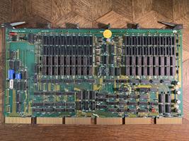
I could not find any information on the board on the internet, but much can be figured out by inspection and testing. First, the board is using 4116 (16Kx1) DRAMs, pretty usual for the era. There is space for 4 banks of 18; each bank would be 16K words (16 data bits plus two parity bits per word.) Here we see two banks populated, minus one of the parity chips. So we'd expect to see 32K words (64 KiB) mappable (or 28K words [56 KiB] with address translation disabled, to accommodate the 4K word [8 KiB] I/O page.) The missing parity chip is unlikely to cause any trouble in this application; in an '11/34, there is no memory parity support without the optional M7850 parity board installed, and this system does not have one.
One of the capabilities of the Unibone is to probe the full 18-bit Unibus address space, looking for active pages. These tests indicated that the memory board as configured was responding to the lower 128 KiB of addresses, even though only 64 KiB was populated. One would suppose that the mapped address range was configured via the DIP switches on the board. Some experimentation with various switch settings yielded the following:
| 7 | 6 | 5 | 4 | 3 | |
|---|---|---|---|---|---|
| 0 | . | . | . | . | 400000 |
| . | 0 | . | . | . | 200000 |
| . | . | 0 | . | . | 100000 |
| . | . | . | 0 | . | 040000 |
| . | . | . | . | 0 | 020000 |
| 4 | 3 | 2 | 1 | |
|---|---|---|---|---|
| 0 | . | . | . | 200000 |
| . | 0 | . | . | 100000 |
| . | . | 0 | . | 040000 |
| . | . | . | 0 | 020000 |
After setting the switches appropriately for the amount of memory physically present, memory test errors went away and the MAINDEC memory diagnostics (excepting parity tests) also ran successfully.
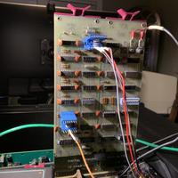
So the Last thing to fix was the problem with the boot monitor at startup. For this, the boot ROM card went back out on an extender so I could get at it with a logic analyzer.
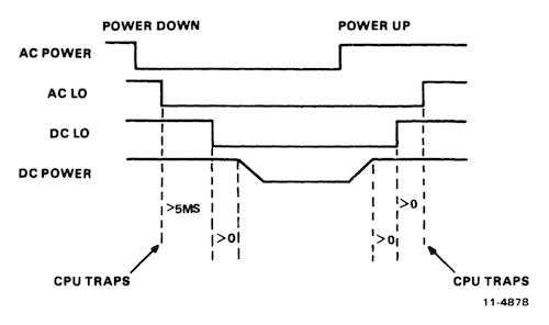
A PDP-11 generates power down and power up traps, through location 024, based on transitions of the AC LO and DC LO Unibus signals. In handling this trap, the processor first reads the PC from location 024, then the PSW from location 026. Many PDP-11s had core memory or battery-backed RAM; this allowed for orderly recovery from power failure events.
PDP-11 boot ROM cards like the M9301 or its younger cousin the M9312 use a hack to obtain control at boot. They monitor AC LO and DC LO, and when detecting a boot condition they jam higher order address bits on the Unibus for a the first couple bus cycles. This causes the PC and PSW to be fetched from locations within the address space of the boot ROM card. Here is most of the circuitry responsible for this:
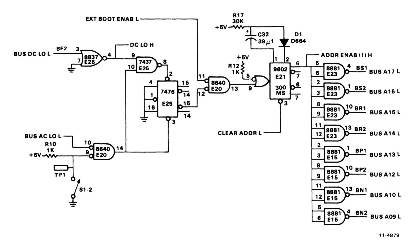
The bus drivers that jam the address bus are seen on the right. The central player here is E21, a 9602 one-shot. CLEAR ADDR L is supposed to arrive after the first two bus cycles (fetch of PC and PSW) and release the bus; the one-shot is set up to timeout after about 300ms and release the bus in any case.
On the logic analyzer, we can see an issue here:

MSYN delimits bus cycles mastered by the CPU. Here we can see that CLEAR ADDR L never arrives, and so the higher-order address bits remained jammed by the M9301 for the full duration of the one-shot timeout. This is okay for the first few instructions, which are executing out of the ROM anyway, but things quickly go awry...
Here is the circuitry responsible for CLEAR ADDR L:
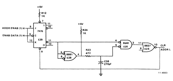
The desired pulse is mediated by 270 uF capacitor C36 in one leg of gate E20, so this is a good thing to check first, and... it is actually missing from the board! (Visible in the M9301 gallery picture above.) Replaced this cap, and now we are in good shape:

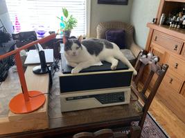
With this, the machine is fully repaired. Spent a little time with it, booting and running various operating systems from emulated storage on the Unibone card. Frieda also approves:
Atari Tempest repairs
Mon 01 March 2021 by Fritz MuellerSome friends of mine own vintage arcade games. Two of them had Atari Tempest machines (one a full-size upright, one the rather more rare "cabaret") that had ceased to play, so I offered to look at them both if they could be dropped off here at my home. Some time later, and here they are in the garage (the Space Duel upright in the background is my own):
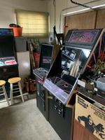
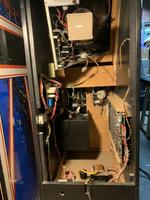
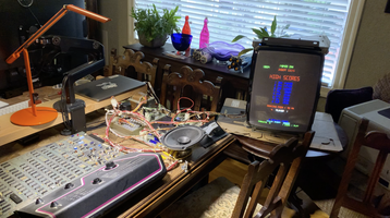
Overall, these are not too complicated, and pretty easy to work on:
-
There is a straightforward linear supply in the bottom of the cabinet, known as the "brick", which provides +10.6 VDC and 50, 36, and 6 VAC.
-
A separate card, the "AR2" (downstream of the brick, also linear), derives +12, +/-5, and +/-22 VDC, as well as hosting audio power amplifiers for game sound.
-
The "brains" of the game are a control board with a 1.5 MHz 6502A processor, ROMs, RAM, and GPIO for settings DIP switches, coin door etc. Since Tempest is a vector game, a fair bit of the control board is also dedicated to vector generation; Tempest uses an "analog vector generator" where vectors are swept by analog integrators with rate inputs fed by DACs. The control board has a daughter-card which has 4x AMD2901 bit-slice ALUs to assist the 6502 with math, and a couple of custom Atari chips ("POKEYs") for sound sound generation and game control input.
-
Last, there is a color vector CRT, the WG6100. This has X and Y deflection amplifiers similar to an oscilloscope, and accepts RGB inputs for color/intensity.
These games are quite common, so all of these components have well-understood failure modes; you will find these discussed in various arcade repair online forums and FAQs. The stuff I always look for:
-
Brick: There is a large electrolytic, known as "big blue", which is the primary filter for the +10.6 VDC. If it is still the '80s original, it is probably worth a check. Modern drop-in replacements are available for ~$15 USD.
There is also a fuse block wired in with crimp quick-disconnects. They are problematic because they may oxidize or rattle loose, causing increased resistance and eventually thermal runaway as the currents here are in the multi-amp range and the brick is located at the bottom of the cabinet where air circulation is not great. It is not uncommon to find toasty wiring and/or melted plastic fuse blocks; if doing repairs in this area I'll generally just clip off the quick disconnect connectors entirely and solder the wires down directly to the fuse block tabs to avoid future reliability issues.
-
AR2: Common fails here are also generally thermal issues. Recap kits for these boards are available from the arcade parts houses, but in my experience aren't often required. Each of the supplies on the AR2 is pretty easy to bench test, but make sure you test with at least a minimal load in place as some of the linear regulators here will behave unpredictably when unloaded. I've never personally seen a failure of the integrated audio amplifiers on the AR2, so I generally don't bother to test them up front; if I have an audio problem with the game I will come back and give them a look later.
The +5 VDC supply here works with a remote sense, which is a matter of some controversy. There can be an appreciable (and variable between cabinets) voltage drop from the AR2 to the game boards over the molex connectors, wiring harness, and game board edge connectors in between. Atari seems to have gone for a remote sense design to automatically compensate for this. The problem is that it is not uncommon for the board edge connectors to loosen over time and/or accumulate dust and oxidation, increasing resistance, and leading to another thermal runaway situation as the supply keeps upping the juice to overcome ever-increasing resistive drop. It is not uncommon to see toasted wiring, toasted AR2, and/or even burnt board traces.
Some techs advocate short circuiting the remote sense at the AR2 (known as the "sense mod") with the argument that it is less destructive to fail into a game-board-under-voltage condition than to fail into an over-current-until-something-burns situation. Others insist the original design is fine as long as board and harness connections are well maintained. I tend to leave things stock unless there is evidence of a problem. If a particular cabinet looks like a chronic +5 burner, though, I'll go ahead and implement the sense mod as well as repairing/replacing the board edge connector; I also add some additional beefy supply and ground wires directly between the AR2 and voltage test terminals on the game boards to shed load off the board edge connector.
For a toasted +5 supply, check Q3, the TO3 series pass transistor on the large heat sink. Sometimes this fails just because of poor thermal connectivity with the heat sink; replacing the stock mica insulator with a silpad and a very thin coat of fresh thermal grease can help here.
-
WG6100 color vector display: This is its own odyssey :-) Lot's of good info on trouble-shooting and repairing these is available on the web. In particular, there is a low-voltage supply section on the deflection board which is quite failure-prone. There are drop-in replacement supply circuits available; you pull all the components in the original section and solder in a small pre-fab daughter board in their place (google "LV-2000"). This upgrade increases the long-term reliability of the WG6100 to such a significant extent that I always opt to install one of these if not already present.
Next most common are fails with the through-hole cable pin connectors. Solder connections here break from repeated mechanical stresses of plugging and unplugging connecting cables, and for some reason the original factory solders here seem pretty shoddy. Always worth giving these a reflow with some fresh solder.
TO3 deflection transistors are mounted off board on the monitor chassis, using the chassis as one big heat sink. These are frequently a casualty of some other cascading failure in the monitor. Flying leads to the sockets holding these transistors sometimes break loose from mechanical stresses, or the old sockets may fail, or mica insulators may develop shorts to the chassis (silpad etc. treatment is generally a good idea here too.)
One thing to be careful of here is that there seem to be a lot of counterfeits of these particular transistors (2N3716/2N3792) on the market. Counterfeits will mostly work, but can exhibit some strange instabilities at cross-over which can manifest as ringing and parasitics in the deflection amplifiers causing "wiggly" vectors that can be difficult to troubleshoot (see pictures from another WG6100 monitor repair immediately below). Make sure to order from one of the larger, more reliable, parts houses for these.
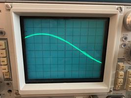
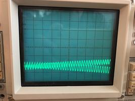
The HV supply in these monitors seems particularly hard on its electrolytic caps; I've seen more cap failures in these HV supplies than anywhere else in these games. Generally worth just doing a recap kit on the HV board if the caps don't look fresh when you get there; it can help improve the stability and appearance of the monitor a lot. After achieving correct and stable B+ on the HV supply, if there still seem to be brightness problems, check C503 on the neck board and refresh if necessary.
-
Game boards: there are eight small PCB mount potentiometers for trimming the analog X/Y outputs. The stock parts are open-frame and seem to collect dust and get twitchy and intermittent (open wiper contacts here can be a cause of loss of video output). I generally just go ahead and freshen these before starting in on the boards, as I hate working with them when they are intermittent/unreliable.
Solder fails in the large interconnect between the mother and daughter boards are also common; these are also worth a preemptive reflow.
These two games from my friends were no exception to the above, and after working the standard stuff for both I had two working bricks, two working AR2s, two working monitors, and one working board set. The second board was producing no output of any sort, didn't appear to respond to its reset switch, and required further investigation.
Okay, like any microprocessor project, start with power, clock and reset... Power looked fine. Clock, not so much. Here's the clock circuit:
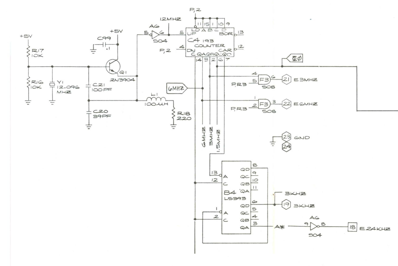
12 MHz crystal with some pulse shaping scoped out fine. Master clock then goes to counter chip C4 to divide down to various derived clocks, including the crucial PHI0 for the 6502. Turns out this counter wasn't counting because its clear input (pin 14, seen arriving from below) was being continuously driven. That input comes from the watchdog circuit and power on reset circuit:
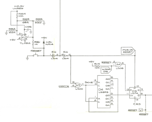
Reset was continuously asserted here because of a dodgy Molex connector which was not delivering +10.6 VDC to TL082 K11 at the left. After fixing this, the machine came out of reset, the reset button was working, and there were signs of activity on the 6502 data and address busses. But the game wasn't really running, and the watchdog was repeatedly timing out, so it seemed to be executing incorrect code.
Pulled the game ROMs, and used a burner/reader to verify their checksums against published values from the arcade game forums (all good). Checked for shorts around the sockets (found none) and reseated the ROMs. Pulled the 6502 and manually drove address bus lines to verify proper operation of the ROM address decoders (all fine). Okay, so time to watch the microprocessor busses on a logic analyzer and see what's going on...
Now, I love my old HP 1660 logic analyzer, lots, but a friend had recently loaned to me a compact 34-channel USB logic analyzer (Intronix LA1034) to see if I might be interested in buying it, and I decided to give it a try for this project. It was pretty easy to probe up the 6502 with a DIP clip, and the software for the analyzer (Windows only) installed and ran without difficulty on my Windows 10 VM.
When the 6502 comes out of reset, it fetches its reset vector from locations FFFC and FFFD, then jumps to that address. Looking at the Tempest ROM listings, the reset vector is supposed to point to address D93F. Watching the 6502 address and data busses, and setting a trigger for address FFFC, we can immediately see a problem:

Here, the top line is the 6502 address bus, and the middle line is the 6502 data bus. The bottom line is the output on the ROM bus, upstream of the driver which gates it onto the data bus.
The 6502 comes out of reset, and attempts reads of locations FFFC and FFFD, as visible on the address bus, but it is receiving incorrect data (C82E vs. the expected D93F). It then jumps to the incorrect address, and from that point onward we are off in the weeds. Interestingly, we can see here that the ROM is, in fact, presenting the correct data.
So the first thing was to try replacing the bus driver between the ROM and the 6502 data busses, but this did not fix the issue (sadness). Besides this and the 6502 itself (already verified by swap with the other working game board) there are only two other drivers on the processor data bus: H2, leading to the daughter board, and F2 leading to the RAM bus. ROM bus seen entering here from the bottom:
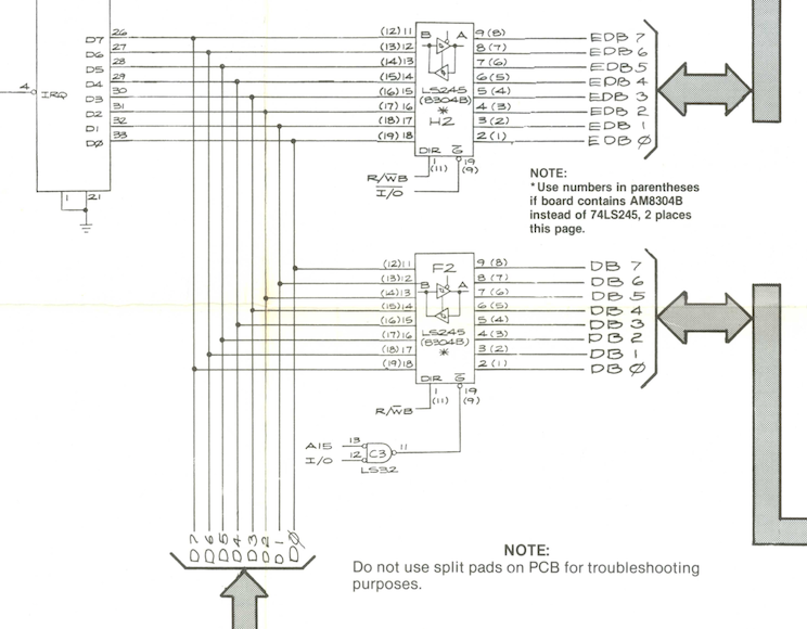
One of these two drivers must be dragging down a couple of lines on the data bus; nothing to do here but try swapping them out one by one. Tried F2 first, and got lucky! Game code began to run, and the game board produced vector outputs. Correct reset sequence after the fix:

From this point forward, just wrap-up:
-
The X positions on the ends of some vectors on the second game board set looked slightly incorrect, beyond what could be adjusted with via the associated rate op-amp offset ("BIP", in Atari-speak) trimmer. This usually indicates a failing rate DAC. Replaced the X rate DAC on this board and the problem was addressed.
-
Various small mechanical repairs to the cabinets, replacement of bits of missing hardware, and cleanup of a hacked-up wiring harness on one of the machines.
-
The cabaret machine had a failed fluorescent tube fixture for its marquee light; after checking with the owner, pulled this and replaced with an LED fixture for greater reliability (I like this one, which is a 120v fixture that doesn't need a separate transformer or supply.)
-
Another upgrade I really like for Tempest machines is a set of brass bushings for the spinner (available here). These make the spinner quiet and smooth as butter.
All done now, and ready to be returned to their owners (after some extensive "burn in" play testing, of course! :-)
Project Genius pyramid puzzle
Fri 26 February 2021 by Fritz Mueller[A catch-up article from Christmas, 2020]
My family knows I have a fondness for puzzles, so my son will typically gift me a few each year at Christmas. Among the puzzles received this year was the Project Genius Pyramid:
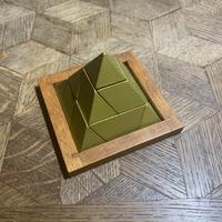
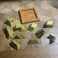
This is pretty entertaining to play with -- since the planes and angles are not orthogonal, the fits of the pieces are less familiar, and I found it more difficult than usual to use "geometry brain" to think ahead while exploring solutions.
I have recently been playing around a bit with Knuth's "Dancing Links" algorithm, described in his paper here. This is a relatively short paper, and if you are unfamiliar with it I'll say I feel it is really worth a read! The gist is a relatively straightforward backtracking algorithm for efficiently finding exact covers of binary matrices, packed with the usual Knuthian tricks and insights. As many classes of problems lend themselves to expression as an exact cover over a set of constraints, the algorithm has broad applications including tiling/packing problems (e.g. Pentominoes, Soma), general n-Queens, Sudoku, logic puzzles, etc. Having coded up an implementation (on Github here), it seemed it would be fun to extend it to explore the pyramid puzzle.
As a tiling puzzle, the first thing to understand was the cell geometry of the pieces and the space to be filled. The base geometry here is an alternated cubic honeycomb, composed of octahedra and tetrahedra. The complex in this case is further sliced into layers which bisect each octahedron, resulting in cells that are tetrahedra and upward- and downward- facing pyramids:
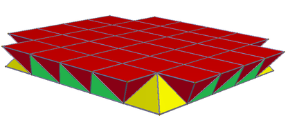
It turns out that the centers of these cells are arranged on a simple rectilinear lattice. The "flavor" (up-pyramid, down-pyramid, tetrahedron) of each cell is simply determined by its position in the lattice; for a cell at coordinates \(x, y, z\):
So, a simple three-dimensional array and indexing scheme may be used to represent the puzzle space, so long as sufficient care is taken with restricting possible piece placements to preserve flavor-invariance.
A further choice of the puzzle makers was to break a symmetry of the puzzle by choosing a layer height such that the cell-center lattice, while rectilinear, is not cubic (the octahedra in the fundamental complex are taller than they are wide/deep, and the tetrahedra are similarly stretched.) I am not sure whether this was done to avoid having the final pyramid look too squat, or if it was done deliberately to reduce the solution space. In any case, this means that we need only consider "right-side-up" and "upside-down" orientations of each piece; the potential "sideways" orientations do not fit the puzzle space.
A final consideration for the solver is restriction to essentially unique solutions by elimination of rotations, refections, and permutation of repeated pieces. This puzzle has some pieces that are chiral without reflected versions, and no repeated pieces otherwise, so reflected and permuted solutions do not exist. To account for rotations, I chose to restrict one piece ("E") to a single orientation (the "E" piece can only appear in solutions in its right-side-up configuration, because if placed upside-down it blocks any other piece form being able to occupy the apex of the pyramid).
These considerations were pretty straightforward to cast into code for the dancing-links solver; a subsequent run quickly produced an atlas of 80 essentially unique solutions. When physically replicating these with the puzzle, it takes a little practice to get used to moving from the rectilinear cell-center space in which the solutions are printed to the isomorphic pyramid/tetrahedron space in which the puzzle physically exists, but this becomes pretty easy once you've played around with it for a bit.
Of the 80 solutions found by the program, only one seems to be generally known on the web, which is the one published by the makers of the puzzle. It is solution 30 as found by the program:
#30:
┌───────────────┬───┐
│ A   A   A   A │ B │
├───────┬───────┤   │   ┌───────┬───┐
│ H   H │ E   E │ B │   │ I   I │ E │
│   ┌───┤       │   │   ├───┐   ├───┤   ┌───┐
│ H │ G │ E   E │ B │   │ G │ I │ F │   │ I │
├───┤   ├───────┴───┤   │   ├───┘   │   └───┘
│ C │ G │ J   J   J │   │ G │ F   F │
│   ├───┴───────┐   │   └───┴───────┘
│ C │ D   D   D │ J │
└───┴───────────┴───┘
For puzzle fans who may own this puzzle, here is an additional challenge based on some inspection of the atlas: some solutions found by the program have a contained sub-puzzle of a smaller pyramid with base 2x3 (in physical puzzle space, where the larger pyramid is considered to have base 3x3.) Can you find any?
Trav-ler 5028 Repair
Fri 26 February 2021 by Fritz Mueller[A catch-up article, documenting events of June/July/August 2020]
Something a little different this time! A friend of mine asked if I could help restore a late-40's portable AM radio set that had belonged to her grandmother:
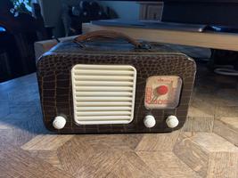
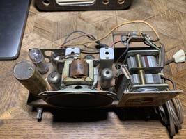
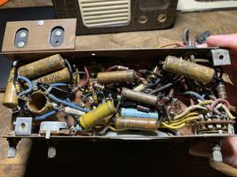
I have done a lot of work with vintage tube instrument amplifiers, so familiar with many of the principles and challenges, but this would be my first radio. So quite a bit to learn!
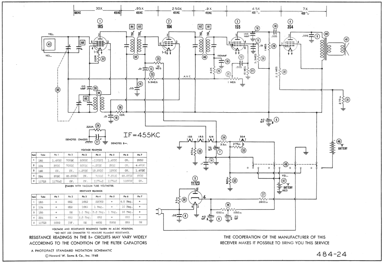
Researching this a little, here is the schematic:
It turns out that there were some very common designs for AM sets in this era, copied and tweaked slightly and produced by many different manufacturers. One cornerstone was the AA5 ("All-American 5"), a five tube superhet design. The tubes had their filaments wired in series, each dropping a bit of the input line voltage, so a power transformer was not required, reducing cost, weight, and size. The lack of a power transformer also lead to some of these radios having a "hot chassis" design, which was not without safety hazards -- more on this later...
There is much information available on the web concerning the theory and operation of the AA5 circuit, and a lot of restoration videos are also available. Interested parties are encouraged to Google, but for the purpose of exposition, I will summarize here in brief. Uninterested parties can scroll a few paragraphs past the indent to pick up the narrative :-)
Following circled numbers from the schematic above, one coil of transformer 44 and one half of ganged tunable capacitor 50 in parallel form a tunable resonant tank. Tube 1 provides gain, and the output is fed back positively via the second coil of transformer 44, forming a tunable oscillator. Antenna 43 and the other half of ganged tunable capacitor 50 in parallel also form a weakly selective tank, which picks up RF and dumps it onto an additional grid of tube 1. Tube 1 is arranged such that the a mix of the two signals (oscillator and weakly selected RF) appears at the plate.
The oscillator and RF thus mixed heterodyne against each other, forming frequency images in the output signal at both sum and difference frequencies; the difference frequencies will be of interest to us here. Since the frequencies in the weakly selected RF and the oscillator track each other, their differences are always centered on a fixed frequency, called the "intermediate frequency", or "IF". The remainder of the circuit need only be concerned with further selection, detection, and amplification at this fixed IF. In this set, the IF has been designed to be 455 KC (KHz).
Transformers 45 and 46, with their integrated capacitors, form cascaded selective bandpass filters at the IF. Tube 2 in-between provides gain and impedance matching between these stages. Tube 3 rectifies (negatively) the now highly selected IF carrier, and cap 18 drains away carrier signal components above the audio range, leaving just the amplitude envelope. Tube 4 provides a final power gain stage at audio frequencies, impedance matched through output transformer 40 to speaker 41.
One interesting refinement here is the "A.V.C." ("Automatic Volume Control"). This taps the detected audio signal and runs it through a long time-constant low pass RC filter, producing a slowly varying DC signal that tracks the audio volume. This is fed back as a bias to the tanks at the front end of the circuit, effectively "turning down" overly strong local stations, so they don't boom out of the radio inconveniently loud compared to more distant stations.
As a portable, this set could be operated off batteries as well as line voltage, but it required two types of batteries: an "A" battery, 1.5V, much like a modern "D" cell, and a "B" battery, 90V, long obsolete. I did not bother with battery support during the restoration.
A lot of the wiring in the radio had rubber insulation, which had hardened and begun to flake away. The wax-covered paper caps all certainly needed replacement, as probably did the multi-section cap in the power supply. One of the tube sockets, supporting a lot of the point-to-point wiring, was cracked and broken. The tuning dial string was broken. There were a few small tears in the speaker cone. Line cord insulation was brittle and broken, and the line cord itself was unpolarized. Rubber grommets holding the tuning capacitor had hardened and shrunk. Given all this, it seemed the best thing to do would be to break down the set completely to better be able to inspect, clean and make mechanical repairs. After this, the Hickock tube tester comes down off the shelf to check the tubes:
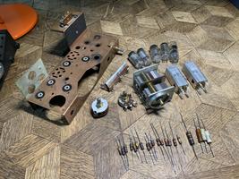
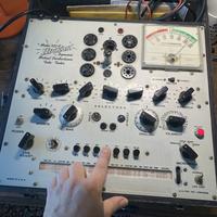
The 117Z3 rectifier was shot. Someone had substituted a 1T4 for the stock 1U4 in the IF interstage. And the 1R5 and 1S5 were weak. Ordered up some replacement tubes, caps, line cord, grommets, and a new tube socket.
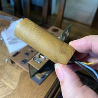
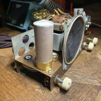
Testing showed that the multi-stage power supply cap was indeed leaky, but I was not able to find a replacement of same dimensions (a 1" outside-diameter tube). I ended up making a replacement with a bit of model-rocketry body tubing, which I stuffed with some modern electrolytic caps of the appropriate values. The result can be seen in the middle picture below, where you can also see some speaker cone repairs done by brushing over the tears with a couple coats of thinned PVA glue. The last picture here shows the completed point-to-point rebuild:
A few words on hot-chassis design and safety: looking at the schematic above, you can see that there is no safety ground, an unpolarized plug, and one side of the AC line is connected through the power switch directly to the B- bus. This means if the line plug is put in one way, B- could be connected directly to AC hot when the radio is on; or if put in the other way, B- would be connected to AC hot when the radio is off, through the resistance of the tube filaments. On some radios slightly older than this, the B- bus is further connected directly to the radio chassis! That means you can get a nasty and dangerous shock off the chassis of such a radio, when the radio is either on or off, depending on which way you plugged in the plug. These radios depended on wooden or plastic cabinets and knobs to keep you from making direct contact with the chassis, but there were still often exposed bolts which connected to the chassis on the backs or bottoms of the cabinets. You were expected to know better...
This Trav-ler radio is a slightly later design, where the chassis is at least isolated from B- by a .1 MFD cap and 220K resistor in parallel. While you won't get such a nasty shock from the chassis of this radio, you can still get an uncomfortable and unsettling "tingle". And if that .1 MFD cap should fail short, your are straight back to danger-ville (on older instrument amplifiers, the capacitor in this particular role became known as the "death cap".)
An improvement for both situations is to replace the line cord with one with a polarized plug, and rewire the radio slightly to a) connect the now known-to-be-neutral side of the line directly to the B- bus, and b) move the power switch to interrupt the hot side of line. EMI filter caps (including the above mentioned "death cap") should be upgraded to modern X or Y safety caps, which are designed to fail open if they fail at all, so as to prevent fire or shock hazard.
Hot chassis designs also pose a challenge (and potential for some surprising moments) with your test equipment. You will often want "ground" for measurement purposes to be B- when working with these things. If this is at or near the hot side of the AC line, and your scope or test gear connects "ground" to safety ground (as most/many do), you are likely to explode the ground lead of your scope probe and/or damage the scope's input amps when you hook it up, with attendant arcs, smoke, and surprise... To reasonably work with hot-chassis designs, you must power them via an isolation transformer, so any point in the circuit under test can "float" relative to the ground of your test equipment. I strongly encourage people unfamiliar with this situation to research it on the web a bit before jumping in on servicing something like this for the first time.
Okay, back to the restoration... After hooking all this up, plugged it in and let it warm up, and while it did come to life and started pulling in AM (!) stations, it was far from optimal. Well, okay, so it needs an "alignment", which means adjusting the tracking on the oscillator and antenna circuits, and tweaking the IF selection transformers to peak up right at design IF. This is done on the bench with an RF test oscillator and a scope or analog meter (topic for another article!) After this, things were better, but there was still a lot of static when tuned in to stations, kind of a granular hiss. So, more research...
It turns out sets like this commonly suffer from something called "silver/mica disease". The IF transformers (45 and 46 on the schematic, the tall silver rectangular parts in the pictures) each have a pair of adjustable coils, and a pair of internally integrated capacitors. The caps in the transformers are typically made with a sheet of mica sputtered with sliver on each side, then sandwiched between a pair of contacts. Both capacitors within the transformer will typically share a single mica sheet substrate. In AA5-like circuits, one of these caps is operating at high potential relative to the other, and over time, dirt and grime provide a path that allows silver ions to migrate between the caps, eventually providing a bridge which rapidly arcs out. As this continues, the mica and silver plating are deteriorated and carbon deposits start to collect accelerating the process.
The cure for this is to open the transformers and remove the deteriorating mica capacitors, then add replacement caps either within the cans or beneath the chassis across the transformer legs. Below you can see some pictures of disassembly of one of the transformers, and the integrated capacitor contact legs at the bottom rolled back out of the way after the deteriorated mica sheet had been removed. Unfortunately, it seems I didn't catch a picture of the damaged mica itself, but a web search will show plenty of similar pictures:
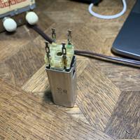
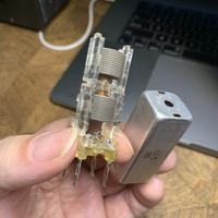
The values of these deteriorated caps cannot be reliably measured, and their design values are not always marked on the schematics. Getting these right to the order of 10 pF or so is important; if they are too far off the available adjustment range of the ferrite slugs in the transformers will be insufficient to properly align the set. A handy approach here is to temporarily tack in some trimmer caps covering the appropriate range. The ferrite cores can then be set in the middle of their excursion, and the set aligned using the trimers; the trimmers are then removed and measured and fixed caps are selected to closely match their set values. An AC bridge is useful for accurate measurement in this range; here you can see a Fluke 710 which was salvaged from the lab:
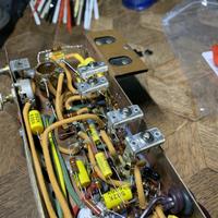
After this final repair and another alignment, the set started to work quite well! I got lucky with timing and managed to pull in some era-appropriate material from Radio Yesteryear on KTRB while I was testing:
This was a really fun project, and I learned a lot along the way -- looking forward to doing a few more like this in the future!