GT40 Terminal
Mon 21 August 2023 by Fritz MuellerA while ago my friend Scott approached me with an idea to collaborate on restoration of a DEC GT40 graphic display terminal of unknown status, belonging to a third collector friend of ours; the idea was to restore the machine to working order for exhibition at the various summer/fall vintage computer shows. The GT40 ran an early (pre-Atari) graphical version of the lunar lander game which was released in 1973. The 50th anniversary of this code seemed a nice theme for the exhibit.
The GT40 was an integrated product consisting of a PDP-11/05 (KD11-B) CPU, a VT11 vector display processor, a VR14 X-Y monitor, a light pen, keyboard, and a DL11 serial interface:
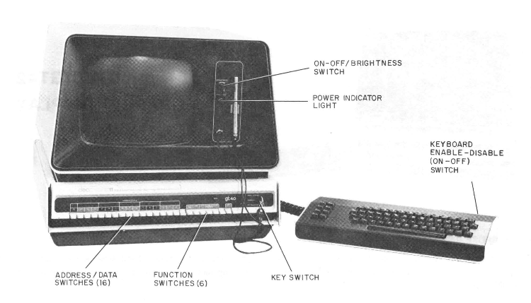
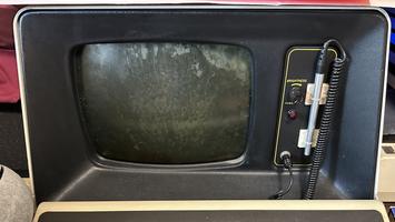
Scott retrieved the terminal, which had a fairly bad case of screen rot. We agreed that Scott would work on restoration of the monitor while I dug in on the system unit. Scott got to work while I dealt with distractions of ongoing home renovations, a ton of work-related travel, and my first bout of COVID (blaargh!)
The screen rot is caused by a deterioriation of a polyvinyl acetate (PVA) layer sandwiched between the front surface of the CRT glass and an outer protective implosion shield. All of this is held together by a retaining ring affixed to the CRT with silicone adhesive. The only fix for this is to disassemble the monitor, separate the sandwich, and clean out and replace the deteriorated PVA layer.
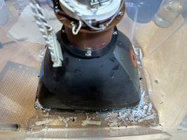
After chatting with some folks who had successfully conducted a similar VR14 restoration at the Rhode Island Computer Museum, Scott obtained some silicone digester to aid in separation of the retaining ring. The terminal was disassembled and then digester was repeatedly injected under the ring with a syringe, allowed to sit, and the resulting softened silicone scraped away over the course of a week.
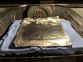
Scott then worked to conform a lexan sheet to the interior of the implosion shield as a replacement for the PVA layer, as RICM had done. This process, conducted in a home oven, proved to be quite fiddly. But persistence paid off, and the end result looks very nice!
After a precautionary reform of the larger power supply electrolytics, careful reassembly, and a gradual bringup on a variac, the monitor showed proof of life on the bench, hooked up to a signal generator source.

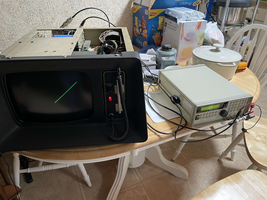
In the meantime, starting to feel better, I began to look at the CPU unit. Power supply electrolytics appeared to be in good shape, and the supply came up on the bench without much difficulty.
The module utilization for this backplane is as follows:
| A | B | C | D | E | F | |
|---|---|---|---|---|---|---|
| 1 | A320 VT40 Display Generator | |||||
| 2 | M7013 VT40 Display Control | |||||
| 3 | M7014 VT40 Bus Control | |||||
| 4 | M7800 DL11 Serial | |||||
| 5 | M930 Term. / UNIBUS out | H214 Core Stack (8K x 16) | ||||
| 6 | G231 Core Memory Driver | |||||
| 7 | G110 Core Memory Control | |||||
| 8 | M7261 KD11-B Control | |||||
| 9 | M7260 KD11-B Data Paths | |||||
On the assumption (later proved wrong) that this was effectively the same as a PDP-11/05 setup, I began debug with just the two CPU cards, an M9301 boot/terminator in position 5A-B, and a grant continuity "knuckle buster" in position 4D. Some problems were immediately apparent from the front console: deposit and examine operations to various memory-mapped CPU registers seemed to work as expected, but when examining contents the M9301 ROM locations bit 13 was always displaying zero. The CPU would not enter run mode, nor could it be single stepped.
Docs suggested that the GT40 would accomodate a KM11 debug module in postion 1B, so in this went. The machine behaved even more strangely when the KM11 was in, hanging up entirely unless the KM11 was put in manual clock mode, and even then stepping microstates at unexpected times. It took a little probing of the CPU clock circuits to discover why:
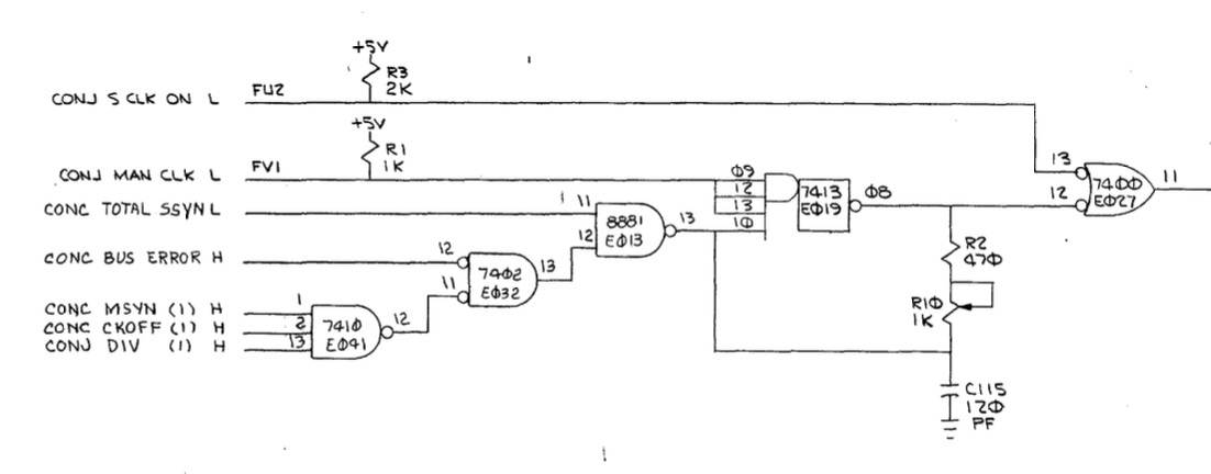
Here we see the RC clock at E019. CONJ MAN CLK L is wired to KM11 switch S2, and inhibits the RC clock when pulled low. With the RC clock thus disabled, NOR gate E027 admits manual clocking via CONJ S CLK ON L, connected to KM11 (momentary) switch S4. The output at E027 pin 11 continues downstream from here as the basis of the main processor clock signal.
As it happened, momentary switch S4 was wired on my KM11 replica with opposite sense from that expected. Thus in its resting postion CONJ S CLK ON L was asserted (low), which meant the clock output at E027 pin 11 was forced constantly high, regardless of the state of the RC clock. This was verified by leaving S2 "off" and pulling S4 over to its momentary position, whence the CPU clock immediately picked up again.
I had never noticed this switch reversal when using the KM11 with the 11/45, the RK11-C, or the 11/34 -- all of these have different clocking circuits unaffected by the default postion of S4. Desoldered and rotated S4 180 degrees, and the problem was fixed.
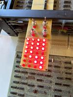
After having addressed this, I single stepped through a few of the console microcode flows and was able to match the microcode listings to what was displayed on the KM11 and the console lights with some success. An action shot of the KM11:
A few tips for anybody else who might be micro-stepping the KD11-B CPU, while we are here:
-
The MPC address displayed on the KM11 is negated -- dark LEDs are ones, and lit LEDs are zeros. This definitely takes a little getting used to...
-
The MPC address displayed on the KM11 is the address of the next micro-instruction, not the current one. This is also pretty tricky until you get the hang of it. One nice thing about it, though, is that the displayed next address does include the wired-or outputs of micro-branches.
-
Each manual clock toggle is one bus clock, and typically, a micro-instruction will take two bus clocks to execute. An exception is the inner part (single shifts) of the micro-flows for shift and rotate instructions, which only take a single bus clock. Generally, it is useful to go ahead and advance two bus clocks at a time, as it is easy to get confused probing for signals that by design aren't clocked until the second bus clock within the micro-instruction.
-
The console lights are hard-wired to always display the ALU B-leg input. Useful intermediate information is often displayed there intentionally by the microcode flows.
Now it was possible to put the data paths board out on extenders and step the microcode for a console examine of a ROM location with bit 13 set, and see why bit 13 never showed up on the console lights. To understand this properly, we need to see an excerpt of the KD11-B data paths:
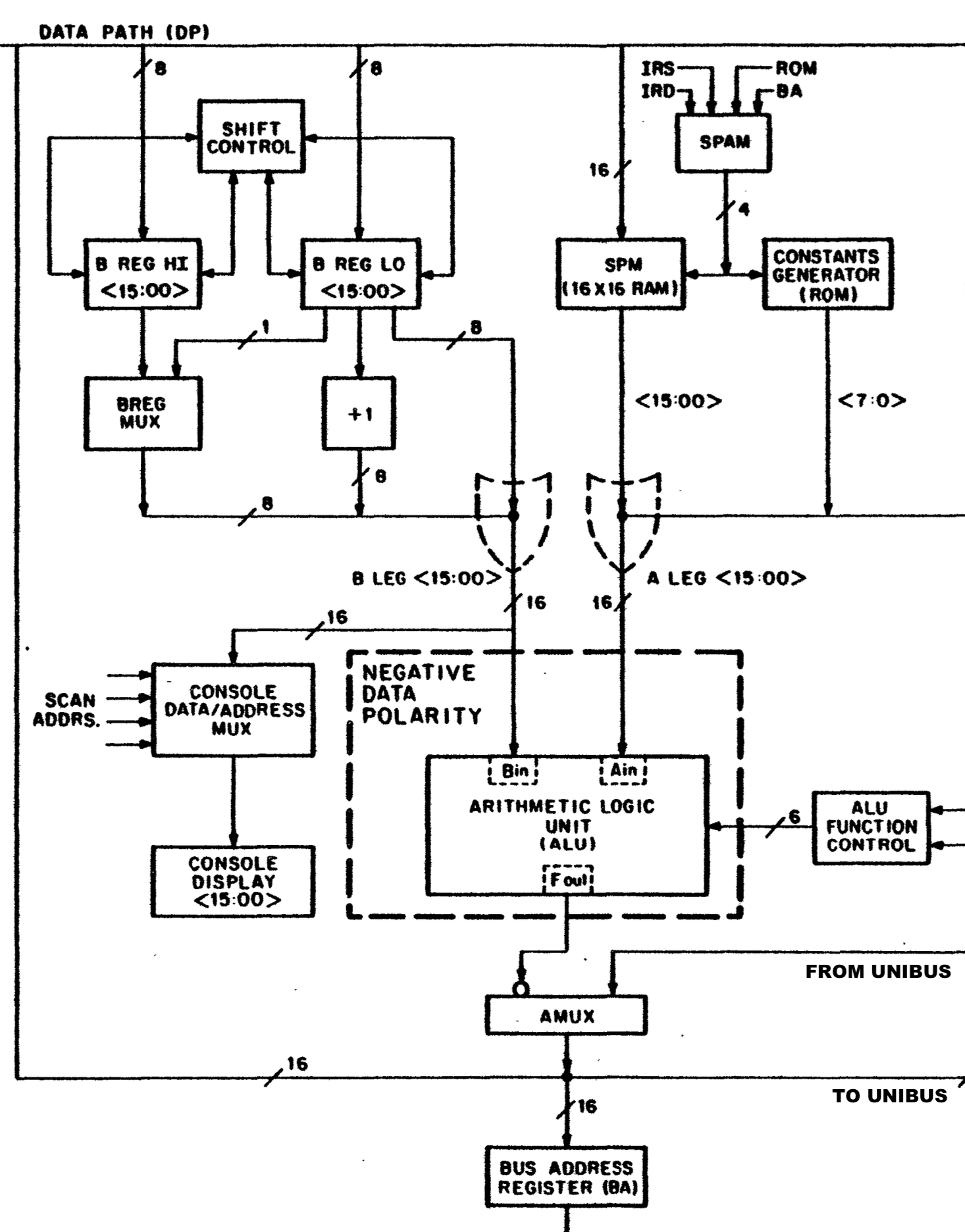
Here you see the ALU in the middle, fed by its B-leg and A-leg inputs. B-leg is fed from the B-register, with provisions for shifting, sign-extension, or forcing the constant +1. B-leg is also continuously displayed on the console lights. A-leg contains, significantly, the 16-location scratch-pad memory (SPM). The first eight locations of this hold processor registers R0 through R7; the remaining eight locations serve as temporary registers for use by the microcode. A-leg can also provide misceallaneous constants from a small ROM.
The A-mux, below the ALU, determines whether the main processor data path is fed from the ALU output, or from the UNIBUS data lines.
With this in mind, the relevant microcode source sequence (taken from the listings in the engineering drawings) is as follows:
LOC  NXT  * CONSOLE EXAMINE SWITCH- FIRST TIME IN SEQUENCE (DON'T INC R[17])
          / GET TO CE1-1 FROM H-2 VIA BUT SWITCH
          / GET TO CE1-1 FROM CE2-2 VIA GOTO
317  307  CE1-1 BA,B←R[17]; BUT SWITCH
          / DISPLAY ADDRESS BY PUTTING INTO THE B REGISTER WHILE EXAMINE IS DOWN
          / LOOP ON CE1-1 UNTIL SWITCH IS RELEASED
307  326  CE1-2 DATI; CKOFF
326  302  CE1-3 B←UNIBUS DATA; GOTO H-2
At micro-location 317 (state CE-1, "console examine 1"), the bus address register and B-register are loaded from SPM location 17, which holds the current console load/examine address. BUT SWITCH ("branch micro-test switch") causes the microcode to loop here as long as the examine switch is depressed. During this time, the fetch address is displayed on the console lights since it has been loaded into the B-register. This was all observed to be functioning normally.
When the examine switch is released, we branch to micro-location 307. Here, a UNIBUS read (DATI) bus cycle is initiated, and the processor clock and microcode execution are suspended until the bus target asyncrohonously asserts SSYN (indicating valid data on the bus) or alternatively times out. The bus cycle was observed to occur normally, leaving SSYN and the correct data (including a correct bit 13) asserted on the UNIBUS.
Proceeding to micro-location 326, we see that the A-mux should be set up there to admit the data from the UNIBUS to the main processor data path and then the B-register should be latched for display. Here a problem was apparent. Sheet DPD of the GT40 engineering drawings covers bits 15:12 of the data paths; package E015 there is an 8266 2x4 mux which implements that slice of the A-mux. E015 was seen via logic probe to be set up with correct select codes and correct input from the UNIBUS. UNIBUS bit 13 was not being correctly passed on to its corresponding output, however -- a failed part.
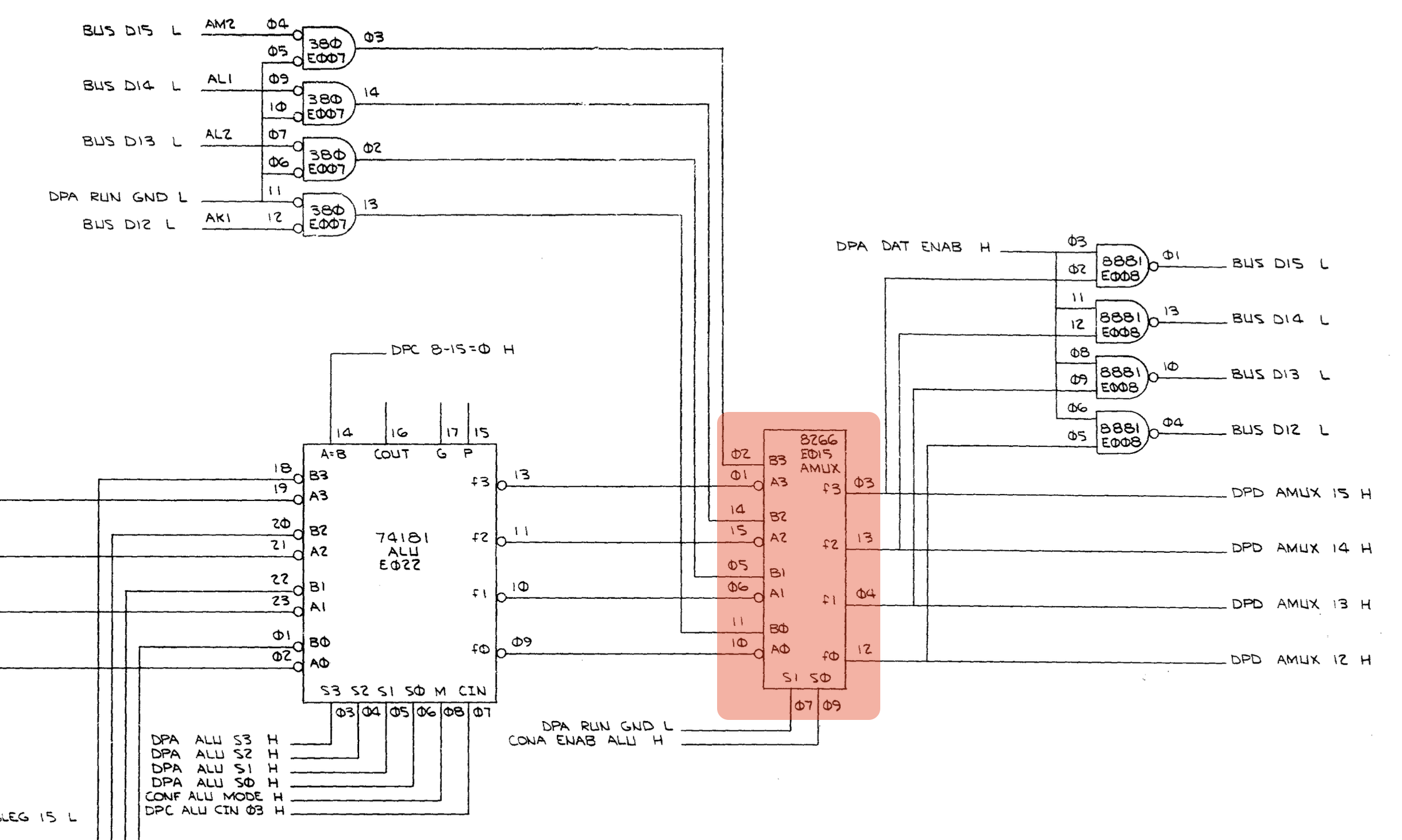
The 8266 is out of production and somewhat rare; for the time being a functioning 8266 was "borrowed" from a spare GT40 data paths board that we obtained from our fellow collector. Removed the bad part, socketed, and replaced with the borrowed part, and the bit 13 display problem was fixed!
Moving next to the run/step problem, the machine was seen to be hanging up in micro-state F-3, after initiating the DATI bus cycle to fetch an instruction. This lead to investigation of some of the the bus control logic, as detailed on sheet CONC of the engineering drawings:

The CPU must negotiate for control of the UNIBUS and assert BBSY if successful. Here I could see the DATI request being successfully latched, but BBSY assertion was blocked at E014 by CONC NPR GRANT H, a non-processor request (DMA) bus grant. Sure enough, some more probing indicated the the processor had issued a NPR grant because it was reading an NPR request over the UNIBUS. Where was that coming from with nothing else in the system?
Well, it turns out in the GT40 the near-side bus termination is integrated onto the M7014 GT40 bus control board that must but in slot 3, so you can't really debug without this card in place! (It could be that an additional M930 terminator in 3-A,B would work, as in a stock 11/05, but I haven't checked the backplane wire list in detail to be certain of this.) In any case, slotted in the M7014, and the machine began to behave much more rationally with a properply configured bus...
Went for broke and slotted in the rest of the display interface boards and (why not?) the core memory and DL11 as well. The machine was showing very promising signs of life. The terminal emulator in the bootstrap ROM ran and was able to render recevied characters on the display! Characters typed on the keyboard were also successfully forwarded out the DL11. A line feed character typed to the terminal emulator seemed to crash it, so that still needed to be looked into. Took the time to toggle in a small test program from the user guide, and this executed correctly rendering a square on the display, indicating most of the logic in the display interface boards was also functioning correctly:
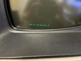
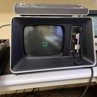
The toggle-in program running above:
1 2 3 4 5 6 7 8 9 10 11 12 13 | 000100 012706 000500 START: MOV #500,R6 ; SETUP STACK
000104 012737 002000 172000 MOV #TABLE,@#DPC ; START VT11 ON TABLE
000112 000001 DONE: WAIT ; LET NPR HAPPEN
000114 000776 BR DONE ; KEEP WAITING IF INTERRUPTED
002000 117124 TABLE: .WORD POINT+INT4+LPOFF+BLKOFF+LINE0
002002 000500 000500 .WORD 500, 500
002006 110000 .WORD LONGV
002010 040200 000000 .WORD 200+INTX, 0
002014 040000 000200 .WORD 0+INTX, 200
002020 060200 000000 .WORD 200+INTX+MINUS, 0
002024 040000 020200 .WORD 0+INTX, 200+MINUS
002030 160000 002000 .WORD DJMP, TABLE
|
Tried to get some program uploads going over the built-in binary loader in the bootstrap terminal emulator, but this didn't seem to be quite working, either. Took a short break for dinner, returned to examine this further, ran for a few minutes, then disaster... Something in the CPU let go, and the machine was once again unable to execute code.
Digging in on this new failure a little, when attempting to single step ROM code from the front panel, the PC was seen to increment by +1 instead of the expected +2; this resulted in an immediate bus error that halted the machine. Back in goes the KM11, then, and the same microcode stepping technique was used to begin investigating.
So how does the KD11-B (ostensibly) increment the PC by 2? It turns out this is done by selecting the PC (SPM location 7) onto the ALU A-leg, constant +1 on the ALU B-leg, and introducing the additional +1 at the carry input of the least significant bit slice of the ALU on sheet DPA of the engineering diagrams:
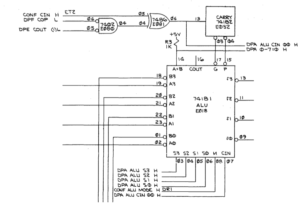
Signal CONF CIN H comes from microcode, wire-or'd with output of operation decode ROMs in the ALU aux control circuitry. In this case, the logic probe revealed that this signal was erroneously low; further investigation revealed that microcode PROM CONF E094 had failed:
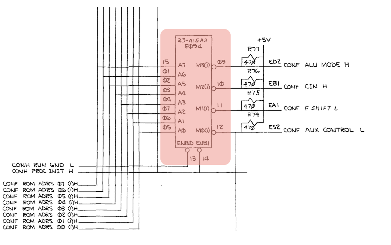
Alright, this is an IM5603 (equiv. 82S126N) bipolar PROM, and I don't happen to have that in stock. So now we're stuck until we can source one. At this point, the day job once again intervened, and I needed to prepare to head off to the Rubin Observatory in Chile for a couple of weeks. Scott came by to pick up the work in progress; had time to share a short demonstration of microcode debug techniques, then off to pack and prepare for my trip...
[ to be continued... ]