PDP-11/45: CPU debug V -- chasing lights!
Sun 19 June 2016 by Fritz MuellerTracked down the source of the inverted result after register-to-register move problem on GRA: outputs of the subsidiary ALU control ROM E74 on pins 6 and 7 are floating. Will need some closer inspection to determine if this is a board fault or a chip fault. In the meantime, I have a spare GRA which I had been reluctant to try because it has a "bad" sticker on it... Decided to give it a try anyway, and it seems to be working much better than the one I have been debugging.
Now have enough of the CPU debugged to toggle in and run a simple light chaser program:
1 2 3 4 5 6 7 8 | 000000 013700 177570 L0: MOV @#177570, R0 ;LOAD COUNT FROM SWITCH REGISTER
000004 005300 L1: DEC R0 ;COUNT DOWN
000006 001376 BNE L1 ;LOOP UNTIL ZERO
000010 006301 ASL R1 ;SHIFT DISPLAY VALUE
000012 001002 BNE L2 ;SKIP AHEAD IF NOT SHIFTED OUT
000014 012701 000001 MOV #1,R1 ;ELSE RELOAD
000020 010137 177570 L2: MOV R1,@#177570 ;STORE TO DISPLAY REGISTER
000024 000765 BR L0 ;REPEAT FROM THE TOP
|
Some notes on the program and video above since I've received some questions:
-
The listing here is shown assembled at location 000000, but the program is relocatable and can be toggled in at any convenient address (000000, on top of the trap vectors, probably isn't the best choice!)
-
Data display should be on "DISPLAY REGISTER" to see the chase.
-
The front panel toggles are loaded into a counter to control the speed of the chase. Without some of the most significant bits set the chase may go too fast to see, especially on older 11's with incandescent indicators. All toggles off is a special case: this will be the slowest chase, since as written the counter wraps around when decremented before being checked for zero. The video has toggles 15 and 14 up.
-
If you look at the address lights in the video, you can see that I ran this program from address 100000. This was because at the time I had a fault in the first 16KW of memory on my MS11-L so I couldn't execute any code at lower addresses.
PDP-11/45: MS11-L debug
Sat 18 June 2016 by Fritz MuellerAfter addressing the -15V problem on the MS11, most of the bad behaviors seem to have cleared up except a stuck (on) bit 6 in the first 16K words of address space (000000-077776). Hooked up the new logic analyzer, and it has been very useful in troubleshooting the board -- can easily capture and inspect the timing of complete memory cycles. Definitely worth the investment!
Using the analyzer, I was able to verify the refresh and chip select logic on the board, then track down the stuck bit to what seems to be a single failed DRAM chip (E96 on the MS11-L engineering drawings). I'd like to test the entire card before ordering replacement parts, but need to set up address translation to get beyond the first two banks from the console.
Here is the address translation register setup that I used for testing. This was followed by a deposit of 000001 to KT11 SR0 (777572) to enable translation. KT11 SR3 was left all zeros to keep D space disabled. This setup allows console access to physical addresses in banks 1 through 7 by appropriate settings of virtual address bits 13 through 15. I wanted to reserve PAR7 to map I/O space, so I left out bank 0 since it was one of the two already tested.
| 772340 | 001000 |
| 772342 | 002000 |
| 772344 | 003000 |
| 772346 | 004000 |
| 772350 | 005000 |
| 772352 | 006000 |
| 772354 | 007000 |
| 772356 | 007600 |
| 772300 | 077406 |
| 772302 | 077406 |
| 772304 | 077406 |
| 772306 | 077406 |
| 772310 | 077406 |
| 772312 | 077406 |
| 772314 | 077406 |
| 772316 | 077406 |
This worked as expected according to panel PROG PHY and the logic analyzer, so the KT11 option which I had not previously tested is at least working for kernel I space. Tested each bank on the MS11 from the front panel using this setup, and uncovered that bank 4 bit 10 also has a stuck on condition. Since bank 1 is working now, I can use that as work space for the time being in order to continue the CPU debug while awaiting some replacement DRAM chips in the mail.
Pics here of the logic analyzer setup, and captured traces of a write and subsequent read to one of the misbehaving chips:


PDP-11/45: MS11-L and CPU debug IV
Sun 12 June 2016 by Fritz MuellerMade some progress on the inverted result after register-to-register move problem: with the help of the KM11, extender card, and a logic probe I was able to track down that signal ALUM L coming onto the DAP is not asserted when it should be for a MOV instruction. This means the ALU is performing in arithmetic instead of logic mode and thus the incorrect result.
I next moved the extender card over to GRA, where this signal originates from a subsidiary ROM, but unfortunately at that point the MS11-L memory behavior got even worse, putting and end to these experiments. So I'll have to tackle that first...
Moved the M792 ROM over to the expansion backplane where the MS11-L resides, and it works fine there. So it doesn't seem to be a bus wiring or jumper problem onto the expansion backplane. Checked the power input pins on the backplane behind the MS11-L. 5V was a little low there; trimmed this up. Probably need to clean or replace the Molex contacts on the power distribution board in the cabinet, as it seems a few mV are being shed there needlessly compared to the output of the same regulator on the main backplane, but things seem within stated tolerances for now.
The -15V input to the MS11-L was missing entirely. Removed the DD11 expansion backplane, and added jumpers between the battery backup supply inputs and the corresponding main supply inputs, per documentation. Now have -15 to the MS11-L, but still no joy.
Will need to go deeper into the MS11-L next time...
PDP-11/45: KM11 replica and CPU debug III
Sat 11 June 2016 by Fritz MuellerReceived the boards and components for the KM11 replica; stuffed and soldered, and it appears to work! There are some photos below. I can easily single-step microcode, clock states, and bus cycles now, which should really help with the CPU debug.
Swapped DAP for a spare, and this has fixed the stuck PC issue. Memory issues remain, but by choosing a working memory range, I can start to toggle in and attempt to execute very simple programs.
The simplest possible program, unconditional branch to self, seems to execute correctly:
1 | 001000 000777 BR .-0
|
A register to register data move test does not however:
1 2 | 001000 010203 MOV R2,R3
001002 000776 BR .-2
|
Control flow is as expected, but the value that ends up in R3 seems to be negated. Still, pretty good progress! Now that I can step machine states, the next step will be to put the DAP out on an extender card and start tracking down signals with a logic probe.
The HP1662A logic analyzer from eBay has also arrived; should come in handy in investigating the memory issue.


PDP-11/45: CPU debug II
Sun 05 June 2016 by Fritz MuellerReceived and installed the replacement lamps for the -15V regulators. Pic below shows what the power supply looks like with all the lamps functioning.
Verified backplane DC voltages and ripple currents again, and re-trimmed all the DC regulators. Verified AC LO and DC LO deasserted and free of glitches. Found some harness wiring mistakes to the DD11 expansion backplane; corrected these.
Tried some CPU board-swaps looking for a quick win, but broken console behavior didn't change significantly with different boards.
Investigated the timing generator board, and found that the crystal oscillator wasn't oscillating. Tracked this down to inductor L1 which looked as if it had been partially sheared away from the board at some point during installation/removal/storage. Repaired this. Success! Able to load addresses from the front console now. Switches are mirrored in the BR when halted in console.
Address bit 0 seems stuck. Swapped PDR from spare board back to the original. Can now examine and modify the light/switch register, and examine the contents of the M792 ROM.
Jumpered the DD11 expansion backplane back in, and slotted in the MS11-L memory. Limited success: can modify and examine memory for example near address 001000, but cannot modify low memory addresses. In some ranges, can only modify every other word. Also, PC seems stuck at 022000.
At this point, I could really use a KM11 maintenance board set. These are pretty hard to get a hold of, but a few folks on the web have built their own reproductions. I put in a PCB order to ExpressPCB with a KM11 layout by Tom Uban (described here), and also put parts on order to stuff it.
Also, figuring I'll need to be going deeper into the CPU debug, I found and bought an HP1662A logic analyzer on eBay, for about the same money as the KM11 PCB and parts!

PDP-11/45: Power fixes and CPU debug
Mon 30 May 2016 by Fritz MuellerConnected up the aforementioned red wire hack to the new power harness, and verified +5V to slots 10 through 15. Console is no longer all address and data lights on, but basic console load address / examine / deposit operations are still not working. A random assortment of address lines seem stuck, different on each power cycle. About the only thing that reliably functions from the console is loading the two highest address bits from the switches immediately after a reset. Pulled the floating point unit, unjumpered the DD11 expansion backplane, and removed all peripherals except the M792 diode ROM; same (broken) behavior...
Scoped all the DC voltages, and did not notice any glitches. Pulled the H742s for some bench work: verified AC LO and DC LO signaling on both units, replaced a broken Mate-n-Lok connector on one of the units, blew out dust from all the 5V regulators and replaced their indicator bulbs with modern equivalent (CM7381). Sourced and put on order a modern equivalent (OL-6003BP) for the indicator bulbs on the -15V regulators.
Next steps will be to verify various Unibus signals on the backplane, then maybe play some swap games with CPU card spares to see if I can get closer to a working console as a starting point. All I have time for this weekend, though; sorry nothing new to see so no new pictures this time!
PDP-11/45: Initial Power On!
Sun 08 May 2016 by Fritz MuellerBeeped out the new harness to check for shorts or incorrect pins, then plugged in just the H742s and fired it up. All the DC regulator modules seem to be working, and I was able to trim them up to nominal voltages at the CPU end of the harness. The indicator lamps on all but one of the DC regulators seem to be burned out, though, so I put some new lamps on order (at last for the +5V regulators; a modern equivalent for the -15V regulators is tougher to find).
Given that success, I plugged in the CPU side of the harness, took a deep breath, and powered on! Hmmm. No detonations or smoke, but all data/address/mode lights lit (see below), which is not right... Front panel lamp test and data address mode switches and indicators are working though at least.
Some investigation on the backplane turned up no +5V to slots 10 though 15, which could be part of the problem. Ah, that's what the mysterious clipped red wire soldered to the backplane might have been about (visible in the top right here...) Sure enough, some inspection shows the corresponding trace on the backplane looks burnt! I could hack this red wire into my new harness I guess, but I'd rather remove it and try to repair the board trace with a shunt. So the backplane will have to come out. I guess that's what I get for not investigating the weird red wire and for not beeping out the power distribution on the backplane before mounting and populating it...
. Well, it's a start!")
PDP-11/45: Power Harness, continued
Sat 23 April 2016 by Fritz MuellerMoved the power modules and partial harness back over to the racks today, got everything remounted, finished and dressed the backplane terminations, and completed the inter-H742 connections.
I did not do the runs for the backplane memory to the lower H742, as I do not have any backplane memory. I probably won't ever have any, either: these memory options are specialized to the '11/45, are quite rare, and only cover part of the available address space. Additionally, they would require me to track down the details of a backplane ECO to do the corresponding parts of the harness correctly. The core and MOS memory that I do actually have are all system-unit options anyway.
Here are some pics of the in-rack wiring in progress, and a couple views of the finished harness. If you add up the capacity of the DC modules, you'll see that an '11/45 like mine (with floating point) is provisioned with +5V at 100 [sic] amps, and -15V at 20 amps. That's no joke of a power supply...


PDP-11/45: Power Harness
Sun 17 April 2016 by Fritz MuellerThe main bit I'm missing from the '11/45 is the power distribution harness; somewhere over the years this was misplaced, or maybe I accidentally gave it away along with some excess '11/40 parts. In any case, I haven't had any luck tracking one of these down (made extra difficult by the fact that my '11/45 is an early model which requires a slightly different harness than more recent models), so I'll have to build one myself from scratch.
Luckily the required harness is pretty well documented in the engineering print sets. The crimp pins are standard Mate-n-Lok still in production. Some of the connectors are out of production, but they haven't been too hard to track down.
Here are some pictures of the amassed wire of appropriate gauges and colors, connectors, crimp pins, and the start of the harness build on the bench:


PDP-11/45: Some parts from eBay
Sat 09 April 2016 by Fritz MuellerI've been keeping an eye on eBay and have collected a few more goodies: a DD11-D nine-slot expansion backplane, a fully populated (128K x 18-bit) MS11-L MOS memory board, and a couple of replacement BC08-R cables for connecting the console to the CPU cards. The MS11-L is a bit of a luxury; I am figuring it will be easier to deal with during bring-up than the core memory systems I have on hand. It will also be nice to run with a full address space.
Below is an updated shot of the CPU chassis with the expansion backplane installed, populated with bus jumpers, terminators, grant continuity cards, the MS11-L memory, a DL11 serial interface, and an M792-YB bootstrap ROM. I've gone ahead and slotted in the FPU in the first four slots, since the cleaned and refurbished CPU cabinet is probably the safest place to store them now. Console cables are also installed:

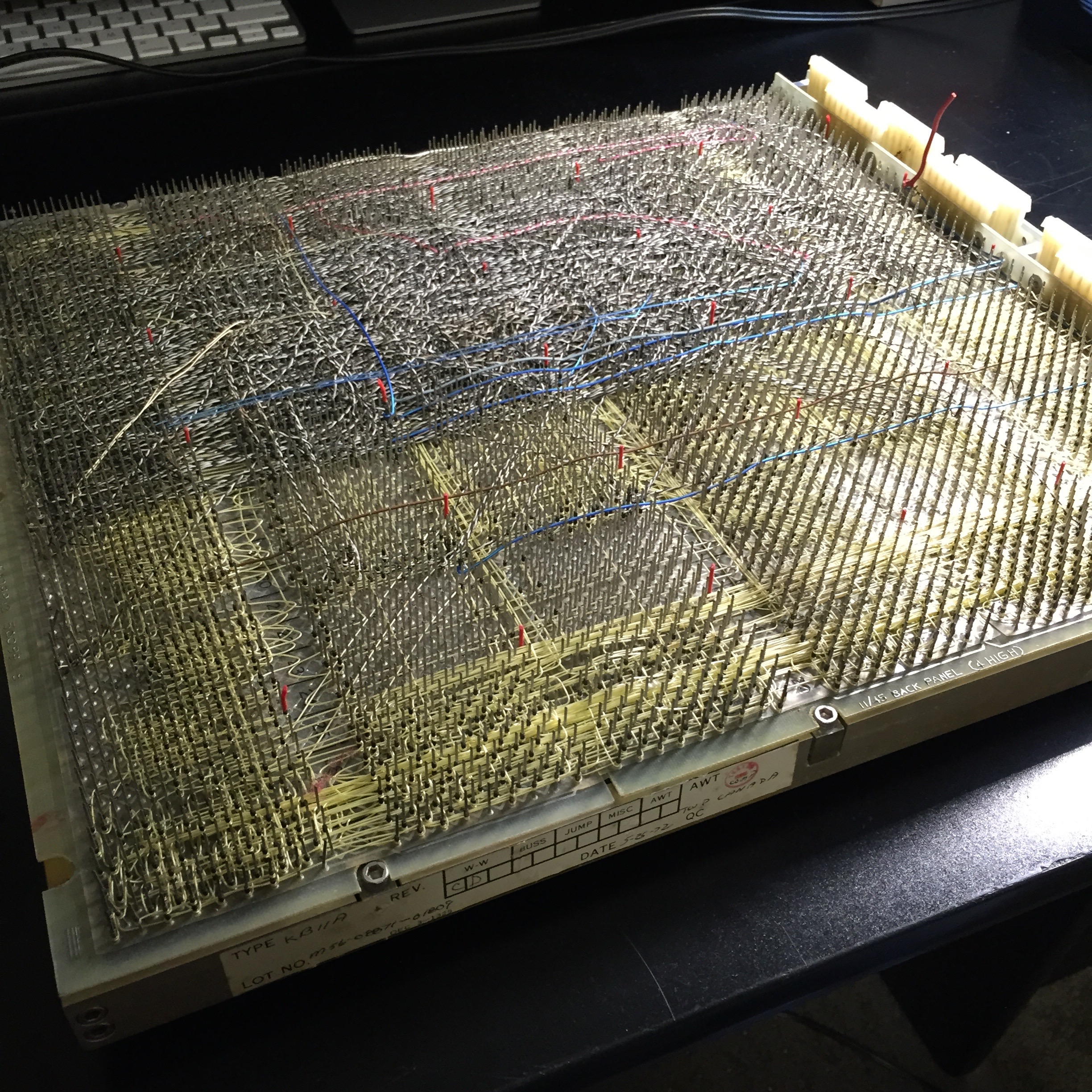
The M792 ROM is an interesting bit, and probably worth a comment. This is a 32-word diode-matrix ROM card. The bits are physically laid out on the card (see pictures below); where there is a diode, there is a logical 1 bit and where there is the absence of a diode there is a logical 0 bit. Typically the matrix would be loaded with a bootstrap program, to save the operator from having to toggle it in from the console on each boot.
The program could be modified by physically adding or removing diodes in the matrix. My card has had such a mod; there is a handwritten note attached from some engineer describing this. The mod customizes the bootstrap to always load from an RK disk unit, to avoid having to toggle in the device address at boot. I will probably revert this mod because I like having things in fairly stock/usual condition.


For fun, here's the source listing of the stock bootstrap. You can match the octal digits of the machine code against the diodes in the ROM above (low word addresses at the top of the matrix, and least-significant-bits on the left).
1 2 3 4 5 6 7 8 9 10 11 12 13 14 15 16 17 18 19 20 21 22 23 24 | 173100 013701 MOV @#177570,R1 ;READ SWITCH REG FOR ....
177570
173104 000005 BEGIN: RESET ;FORCE CLEAR IF RETRY
173106 010100 MOV R1,R0 ;....DEVICE WC ADDRESS
173110 012710 MOV #-256,@R0 ;SET TO READ 256 WORDS
177400
173114 020027 CMP R0,#177344 ;IS IT DECTAPE?
177344
173120 001007 BNE START ;NO. GO TO START
173122 012740 MOV #4002,-(R0) ;YES. MOVE TAPE TO FRONT
004002
173126 005710 TST @R0 ;WAIT FOR ERROR!
173130 100376 BPL .-2
173132 005740 TST -(R0) ;IS IT ENDZONE?
173134 100363 BPL BEGIN ;NO. TRY AGAIN
173136 022020 CMP (R0)+,(R0)+ ;ADJUST POINTER
173140 012740 START: MOV #5,-(R0) ;NOW START ACTUAL READ
000005
173144 105710 TSTB @R0 ;WAIT FOR DONE
173146 100376 BPL .-2
173150 005710 TST @R0 ;ERROR ENCOUNTERED?
173152 100754 BMI BEGIN ;IF SO START OVER
173154 105010 CLRB @R0 ;FOR DECTAPE,STOP TRANSPORT
173156 000137 JMP @#0 ;GO TO ROUTINE LOADED
|
Hmmm, the Pygments syntax highlighting package used by my blog generator doesn't seem to grok MACRO-11; may have to do something about that...