PDP-11/45: Diagnostics XI - FP11 FPU, cont.
Sun 23 October 2016 by Fritz MuellerWrote some small test programs to investigate FP add/subtract. Turns out that single-precision add/subtract works fine, but double-precision results come back with some erroneous bits set in the fraction. Here's the test code I ended up using for troublshooting -- when executed on my machine, bits 24 and 25 end up incorrectly set in the result at D3:
1 2 3 4 5 6 7 8 9 10 11 12 13 14 15 16 17 | 000000 AC0=%0
000001 AC1=%1
000000 .ASECT
001000 .=1000
001000 170011 START: SETD ;SET DOUBLE PRECISION MODE
001002 172467 000014 LDD D1,AC0 ;FETCH FIRST ADDEND FROM D1
001006 172567 000020 LDD D2,AC1 ;FETCH SECOND ADDEND FROM D2
001012 172100 ADDD AC0,AC1 ;ADD THEM (RESULT IN AC1)
001014 174167 000022 STD AC1,D3 ;STORE RESULT TO D3
001020 000000 HALT
001022 040200 000000 000000 D1: .WORD 040000,000000,000000,000000 ;0.5
001030 000000
001032 040200 000000 000000 D2: .WORD 040000,000000,000000,000000 ;0.5
001040 000000
001042 000000 000000 000000 D3: .WORD 000000,000000,000000,000000
001050 000000
001000 .END START
|
So, the usual procedure: KM11 in the floating point slot, and FRL (where these bits are handled) out on extenders. First step is to verify the microcode sequencing with the KM11 and front panel, and it looks good. In particular, the FPU is sequencing through states ADD.04 and ADD.06 per expectation for double-precision, branching correctly for non-zero operands, and taking the equal exponents branch through ADD.24 (refer to page FLOWS 8 of the FP11 engineering drawings).
Next, stopped in state ADD.38, where the fraction addition occurs, and scanned the inputs and outputs of all the 74181 bitslice ALUs with a logic probe. Bit 28 of the A input to the FALU (E16 pin 2, refer to page FRLJ of the FP11 engineering drawings) is incorrectly set. This is arriving via the AR register.
The value in the AR register is originally fetched from the register scratchpad, then flows through QR, BR, and the FALU during microstates ADD.04, ADD.06, and ADD.02. Some more stepping and logic probe work showed that the fraction values are correct along these paths through these states. So it looks like AR itself may be at fault.
Set up the logic analyzer on E15, which is a 74194 shift-register that holds bits 28-31 of AR. It looks like it is indeed faulty:
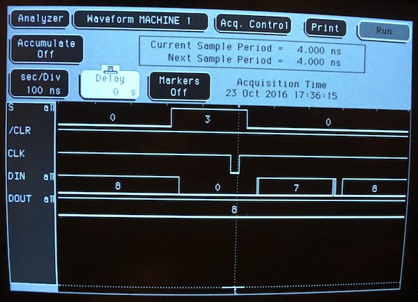
Here we can see what should be a broadside load: positive CLK edge, S0 and S1 both asserted, and inputs of all zeros. But the output sticks brokenly at 8. Pulled this shift register, soldered in a socket, and put a replacement and a couple of spares on order. All for now, until the parts arrive.
PDP-11/45: Diagnostics X - FP11 FPU, cont.
Sat 01 October 2016 by Fritz MuellerOkay, here's the dig in on the FP11 STST diagnostic failure. As detailed previously, I'd been seeing an incorrect FEC after executing a small test program to generate a minus-zero condition. I'd verified that the microcode sequence was per expectation, and that the correct FEC was being stored and retrieved from AC7[1:0] in microstates TRP.50 and the start of TRP.60.
The end of TCP.60 and all of state TRP.70 are used to move the FEC and FEA from AC7[1:0] to AC7[3:2] via QR and BR, and something was going awry here. Since the nominal FEC is octal 14, I decided just to trace the four least significant bits. Consulting the engineering drawings, the nominal flow of these bits through logic on the FRL during these states would be:
| Function | Package | Dir | Pin:Level | Microstate | |||
|---|---|---|---|---|---|---|---|
| ACi<03:00> | E85 | out | 11:H | 9:H | 7:L | 5:L | TRP.60 (2) |
| QR<06:03> | E74 | in | 3:H | 4:H | 5:L | 6:L | |
| out | 15:H | 14:H | 13:L | 12:L | TRP.70 (3) | ||
| BR<07:04> | E75 | in | 13:H | 12:H | 4:L | ||
| out | 15:H | 10:H | 2:L | ||||
| BR<03:00> | E87 | in | 5:L | ||||
| out | 7:L | ||||||
| FALU<07:04> | E77 | in | 20:H | 22:H | 1:L | ||
| out | 11:L | 10:L | 9:H | ||||
| FALU<03:00> | E89 | in | 18:L | ||||
| out | 13:H | ||||||
| ACMX<03:02> | E83 | in | 13:L | 3:L | |||
| out | 9:L | 7:L | |||||
| ACMX<01:00> | E84 | in | 13:H | 3:H | |||
| out | 9:H | 7:H | |||||
| ACi<03:00> | E85 | in | 12:L | 10:L | 6:H | 4:H | |
Note that the bit values are inverted here by the FALU, since the reigster file used on the FP11 has inverting outputs.
Threw the FRL out on extenders and starting verifying the chart above with a logic probe. Surprisingly, everything probed out correctly (?!) Reset and ran the test program and verified that the bug had gone away. Hmmm... My only guess here is that there was some dust or a whisker shorting some of the pins that I dislodged with the logic probe, or perhaps an oxidized board conection. In any case, it seems to work robustly now. Of the FP11 diagnostics, the following now pass:
| Diagnostic | Description | Status |
|---|---|---|
| CFPAB0.BIC | LDFPS,STFPS,SETI,SETL,SETF,SETD,CFCC | pass |
| CFPBB0.BIC | STST | pass |
| CFPCD0.BIC | LDF,LDD,STF,STD | pass |
| CFPHB0.BIC | CLR,TST,ABS,NEG | pass |
| CFPKB0.BIC | LDEXP | pass |
CFPDB0.BIC, which tests floating point adds/subtracts, is failing. All for now -- on to debugging add/subtract next time...
PDP-11/45: H720E teardown and inspection
Sun 18 September 2016 by Fritz MuellerStarted in on the H720E power supply that is part of RK05 storage system. Just initial teardown, cleaning, and inspection for obviously failed parts. Looks pretty good, though there is a lot of dust and grime because this unit lost its top cover plate somewhere over the years (I'll have to build some sort of replacement).
There are a couple of 22,000 mFD 50v electrolytic caps here that I'll try reforming before hitting them at full power, since they've been sitting idle for upwards of 30yrs! Also, one obviously leaking 330 mfd axial on regulator board, so I'll replace this and all its identical twins. Parts on order...


PDP-11/45: Diagnostics IX - FP11 FPU, cont.
Sat 10 September 2016 by Fritz MuellerDid a lot of reading on the FP11 design. A few interesting notes that are buried in the maintenance manual:
-
When debugging FP11 microcode with a KM11 in single-microstep mode, the 11/45 front panel microcode display shows the address of the next microinstruction, NOT the current microinstruction. This is because the stop-point for single microinstruction is at a point between T2 and T3, just after the next microinstruction addr has been calculated. This is different behavior than the 11/45 CPU front panel microaddress display.
-
There's a note in the maintenance manual that explicitly cautions that when using extender boards for debug, the RC maintenance clock should be used, and set with period >50ns. I had not been doing similar while debugging the KB11-A CPU, and maybe this explains the occasional different behavior I'd see when throwing boards out on extenders... In particular, I had seen this when debugging a spare CPU GRA; next time I return to that board I will try the CPU RC clock.
Okay, so here's my first simple test program for STST:
1 2 3 4 5 6 7 8 9 | 000000 AC0=%0
000000 .ASECT
001000 .=1000
001000 170127 044000 START: LDFPS #044000 ;FID+FIUV
001004 172467 000004 LDF NEGZ,AC0 ;LOAD A MINUS-ZERO
001010 170300 STST R0 ;STORE FEC TO R0
001012 000000 HALT
001014 100000 000000 NEGZ: .WORD 100000,000000 ;MINUS-ZERO
001000 .END START
|
This would be expected to produce the 000014 "Floating Undefined Variable" (minus-zero) exception code in R0, but I see an incorrect value of 177417. Using the KM11 on the FPU shows the -0 trap and STST microstate flow is per expectation.
Put the FRL out on the extender and started stepping the microcode, examining the state of the pins at the AC register file along the way. In the -0 trap flow, the FEC code 000014 presented (inverted) at TRP.50 via the EALU, and subsequently retrieved at TRP.60 looks correct. However, the value presented at TRP.70 via QR, BR, and the FALU does not. Out of time this weekend; Will have to chase signals back through those paths next time!
PDP-11/45: Diagnostics VIII - FP11 FPU
Sat 03 September 2016 by Fritz MuellerSlotted in FP11 spares that I hadn't tried previously, and this has produced some improved results -- returning to diagnostic CKBME0 (11/45 traps) this now passes with the floating point installed. Additionally, diagnostic CFPAB0 passes.
CFPBB0 and CFPCD0, however, are failing. Unfortunately, the source code for these is not available in the PDP-11 diagnostics database at retrocmp. The names of the diagnostics tell which instructions they are testing, though. CFPBB0 is annotated as testing the STST instruction. Rather than work through disassembling the rather lengthy diagnostics, I'll probably just write some simple test programs around the STST instruction for next time. In the meantime, I'll do some reading on the FP11 in preparation for microcode-step debug.
PDP-11/45: Diagnostics VII - KT11 MMU
Sat 13 August 2016 by Fritz MuellerMoving on to the KT11 MMU: running the first diagnostic in the CKT suite, got error reports at 010340, 010560, and 011000. Consulted the diagnostic listings, and these particular tests have to do with D-space translations from kernel, supervisor, and user modes. The D-space logic is largely on module SSR, so I swapped this out for a spare. After that, I was able to pass the full suite of basic MMU tests:
| Diagnostic | BEL | Description | Status |
|---|---|---|---|
| CKTAB0.BIC | 017412 | KT11-C basic logic part 1 | pass |
| CKTBC0.BIC | 015674 | KT11-C basic logic part 2 | pass |
| CKTCA0.BIC | 023304 | KT11-C access keys | pass |
| CKTDA0.BIC | 016360 | KT11-C MTPD and MTPI | pass |
| CKTEB0.BIC | 015310 | KT11-C MFPD and MFPI | pass |
| CKTFD0.BIC | 016422 | KT11-C aborts | pass |
Put the failing SSE module in the repair queue along with the other failed spares I've identified along the way, and will return to troubleshoot/repair it later. For now, things are looking pretty good with the CPU! I still need to run and pass the more heavyweight diagnostics: the 11/45 instruction exerciser, KT11 exerciser, and MS11-L exerciser. All three of these still seem to have halts, but they are quite complicated diagnostics in comparison to the rest, making use of additional peripherals, etc. I'll need to study these a bit before I can be sure I am using them correctly. I have also skipped the power fail diagnostics for now as I will need to restore some core memory in order for these to work correctly.
Next up will be to work on the FPU...
PDP-11/45: Diagnostics VI - GRA ALU PROM repair
Sun 07 August 2016 by Fritz MuellerData I/O Series 22 PROM programmer from eBay showed up, as well as some unprogrammed Signetics 82S123. Punched in the subsidiary ALU control ROM contents from the listing on GRAK in the 11/45 engineering drawings and burnt a new PROM. Put a socket and the new PROM in place of the failed part on my original GRA, slotted it into the CPU, and success! Diagnostic CKBOA0 now passes. I will probably return to the other faulty GRA at a later point, as it is partially diagnosed and I like to have spares working and ready to go.
Next time I'll be moving on to the CKT series of tests for the KT11 memory management cards...


PDP-11/45: Diagnostics V - D0AA0-D0MA0, CKBOA0
Sun 31 July 2016 by Fritz MuellerThe day gig has been keeping me pretty busy for the last couple of weeks, but had some time to work on the PDP-11 again this weekend, so here's an update.
Looking a little deeper at the diagnostics database over on retrocmp.com, I realized that I had skipped the entire set of generic 11-family "D0" tests. Downloaded and ran these via PDP11GUI and they all passed. BEL character patch locations, as described previously, are summarized here for future reference:
| Diagnostic | BEL | Description | Status |
|---|---|---|---|
| D0AA0.BIN | 014212 | Branch | pass |
| D0BA0.BIN | 004336 | Con branch | pass |
| D0CA0.BIN | 005526 | Unary | pass |
| D0DA0.BIN | 016370 | Binary | pass |
| D0EA0.BIN | 010562 | Rotate/shift | pass |
| D0FA0.BIN | 017224 | CMP equality | pass |
| D0GA0.BIN | 013650 | CMP non-equality | pass |
| D0HA0.BIN | 013434 | Move | pass |
| D0IA0.BIN | 014126 | Bit set clear test | pass |
| D0JA0.BIN | 007472 | Add | pass |
| D0KA0.BIN | 007124 | Subtract | pass |
| D0LA0.BIN | 015722 | Jump | pass |
| D0MA0.BIN | 003250 | JSR RTS RTI | pass |
Of the "CKB" series of tests, CKBOA0 (11/45 states) is the only one I that is not yet passing. Looking into this a little further, the first failing sub-test is T65:
1 2 3 4 5 6 7 8 9 10 11 12 13 14 15 16 | 010540 010701 T65: SCOPE ;
010542 012737 030000 177776 MOV #PUM,@#PSW ;KERNEL MODE, PREV USER MODE
010550 012706 000500 MOV #KPTR,KSP ;SET KERNEL STACK POINTER
010554 012716 000700 MOV #UPTR,(KSP)
010560 106606 MTPD USP ;SET USER STATCK POINTER
010562 005067 170110 CLR UPTR-2
010566 052737 140000 177776 BIS #UM,@#PSW ;USER MODE, PREV USER MODE
010574 106506 MFPD USP ;PUSH USER STACK POINTER ONTO USER STACK
010576 042737 140000 177776 BIC #UM,@#PSW ;KERNEL MODE, PREV USER MODE
010604 106506 MFPD USP ;PUSH USER STACK POINTER ONTO KERNEL STACK
010606 022716 000676 CMP #UPTR-2,(KSP) ;CHECK THAT USER STACK POINTER WAS
010612 001401 BEQ .+4 ;PUSHED PROPERLY (ONCE)
010614 000000 HLT ;ERROR!
010616 022767 000700 170052 CMP #UPTR,UPTR-2 ;CHECK THAT USER STACK POINTER IS ON THE
010624 001401 BEQ .+4 ;USERS STACK
010626 000000 HLT ;ERROR!
|
This runs amok on the MFPD instruction at 010574, which should push the user stack pointer onto the user stack. Instead, the user stack pointer is pushed to memory at an incorrect address; 010676 instead of 000676. This actually overwrites subsequent test code. Since the value pushed is 000700, a hard-coded loop is created that prevents the test from completing the pass even if resumed from halt.
The relevant states in the microcode flow here are MFP.80, MFP.90, and MFP.10:
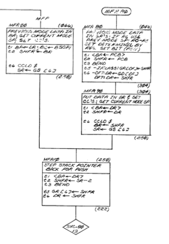
Stopping at T2 of MFP.10 using the KM11, I can see that the correct value 000700 was fetched to DR (as displayed by the console address lights), but the incorrect value of 010676 is appearing at the output of the ALU/shifter (as displayed by the console data lights when set to data paths). Throwing the DAP card out on extenders and taking a look around with a logic probe revealed that the errant bit 12 is sourcing from the ALU. At each slice of the ALU, function selectors S3-S0 are correct, CIN is correct, and overall B-mux constant value "2" is correct. The errant bit is arriving to the ALU from the A-mux...
Chasing this upstream, A-mux selectors S1,S0 are correct, but the bad bit arrives to the mux input on GRAH SR12. Hmmm, maybe this is one of the things the "BAD" sticker on the GRA is referring to... Next step is to throw the GRA on the extender, and chase the signal back towards SR and the register files. However, here I hit a snag: the M9301 monitor does not run correctly when the GRA is on the extender! That's pretty weird. Some investigation with the KM11 and some hand-toggled instructions revealed that at least the Z status bit is not set correctly/reliably when the card is on the extender. Some of the Z bit logic lives on the GRA also, so I can take a look at that, but I am now out of time for this weekend. Next time!
A few other miscellaneous notes in wrap-up:
-
I have been running with the spare GRA marked "BAD" because the first GRA I was using turned out to have a failed ALU subsidiary PROM. In the meantime I tracked down a PROM programmer and some compatible parts on eBay -- these should arrive sometime this week at which point I should be able to repair the original board and give it another try.
-
The uPB feature of my home-brew KM11 really doesn't work quite right. It often stops the machine at the requested micro-state but on the wrong instruction (skipping the first occurrence of the target state seemingly). This caused me a great deal of confusion today, as I was stepping through flows at a different program location than I had assumed, until I finally noticed the address lights on the console.
-
ESC key on the VT52 is non-functional, making it impractical to use for RT-11. The key mechanism looks okay from the top (thanks for more helpful advice from the vcfed forum!). I think I'll need to pull the keyboard PCB and re-flow the solder on the affected mechanism as a next step.
-
Looking forward to checking out Vintage Computer Fest West sometime next weekend!
PDP-11/45: Diagnostics IV - CKBME0
Sun 17 July 2016 by Fritz MuellerSome progress with the CKBME0 diagnostic mentioned previously. It seems the concern with how the test behaves wrt. preconditions of the serial interface was well founded.
In order to debug more easily, I extracted the failing test and built a small loop around it, with a pass counter and display register update, etc. In the original test suite, a RESET instruction is executed immediately prior to the failing test, and it takes some time to come around the failing test on each pass, so I included a RESET and a delay loop in my test code as well. I then got failure modes and rates consistent with the original test suite.
The experiments previously described had indicated timing sensitivity (e.g. running on the RC maintenance clock at 50% clock speed changed the pass failure rate from ~50% to 100%) so I began to think more seriously about timing between the processor and the serial card, and how the time taken to circulate the entire suite of tests could affect the precondition of the serial interface when entering the test in subsequent passes. A re-read of the DL11 documentation showed that the transmit data is also double-buffered; if the transmit shift register is empty, a character written to the output buffer will be latched to the transmit shift register causing the output buffer to go ready again almost immediately.
I inserted the following code before the BIS/WAIT sequence in the original diagnostic (listed previously), which establishes consistent preconditions (shift register full, buffer empty) before the BIS. Success rate went to 100%:
1 2 3 | MOV #40,@#177566 ;ENSURE XMIT SHIFT REGISTER HAS SOMETHING TO CHEW ON
L0: TSTB @#TTCSR ;CHECK XMIT BUFFER
BPL L0 ;LOOP UNTIL READY, ENSURES INT IMMEDIATELY AFTER BIS
|
I then further verified that the unmodified original diagnostic suite passes 100% if I turn the M7800 down to 4800 Baud. Worth noting when trying to run these older diagnostics!
PDP-11/45: VT52 repair
Sat 16 July 2016 by Fritz MuellerReplacement oscillator arrived for the VT52, so spent some time getting it back going again. Things got much better with a stable timing chain, but some glitchiness remained -- tracked this down to the socketed microcode ROMS which just required a reseat.
Here you can see the new oscillator fitted (silver rectangular can with tie-wrap). The microcode ROMS are the four socketed chips towards the right in the picture. Interestingly, the schematic I have calls for 8 ROMS of half the size of the ones that are in here, and indeed you can see the unpopulated spaces for these on the board.
