PDP-11/45: V6 Unix Troubleshooting
Sat 24 October 2020 by Fritz Mueller[A catch-up article, documenting discoveries of Jan/Feb 2019]
In early 2019, I made a V6 Unix pack from the Ken Wellsch tape image, as mentioned in this blog
entry. It booted on my machine, but dumped core on the first ls in single-user
mode, or as soon as I did any heavy lifting in multi-user mode.
The following is the first part of a chronology of the troubleshooting campaign that took place over the next month and a half, culminating in a smoking gun hardware fix and successful operation of V6 Unix on the machine. This was largely a collaborative effort between Noel Chiappa an myself via direct email correspondence, though help was received from others via the cctalk mailing list as well.
January 8-9
Initial experiments. Described the ls crashes to Noel. He theorizes that ls works in one case and
crashes in another is because it lands in a different spot in memory in each case.
Luckily, a subsequent od on the core file does not crash, and a core file is successfully extracted:
140004 000000 141710 141724
$DK
@rkunix
mem = 1035
RESTRICTED RIGHTS

Use, duplication or disclosure is subject to
restrictions stated in Contract with Western
Electric Company, Inc.
# LS
MEMORY FAULT -- CORE DUMPED
# OD CORE
0000000 141552 141562 000000 000000 000000 000000 000000 000000
0000020 000000
0000060 000000 000000 000000 000001 000000 000000 063260 140076
0000100 001700 000000 000104 066112 067543 062562 000000 000000
0000120 000000 000000 000000 060221 000567 067543 062562 000000
0000140 000000 000000 000000 000000 066112 000000 000020 000000
0000160 000000 000000 000000 000000 177701 000000 000020 000000
0000200 000000 000000 000000 000000 177701 041402 016006 000000
0000220 000000 000000 000000 000000 066016 041402 016006 000000
0000240 000000 000000 000000 000000 066016 075120 075120 075120
0000260 000000
0000300 000000 000000 000000 000000 000013 010400 001050 002366
0000320 000000 000104 000035 000024 000000 141732 141742 141664
0000340 141674 000000 000000 000000 000000 000000 000000 000000
0000360 000000
0000400 000000 000000 000000 000000 000000 000000 000012 000000
0000420 000000 000000 000000 141772 000000 000000 000000 000000
0000440 000000
0001500 000000 025334 003602 001236 025334 003602 002454 003602
0001520 063260 177716 000000 141542 016070 001176 000000 003602
0001540 063260 177716 000000 141562 016070 001176 066352 030300
0001560 063260 025334 003602 077572 000013 107564 141626 000512
0001600 000000 141604 141616 000300 074616 025334 003602 000217
0001620 000203 107404 020276 000512 000000 141634 141640 003602
0001640 000007 000135 107454 141662 014314 003602 066352 005674
0001660 000000 141712 013640 074616 000000 001000 000000 000000
0001700 001000 074616 063260 066352 000013 141726 023730 066352
0001720 063260 000000 000013 141742 023502 003602 000000 177760
0001740 000013 141756 022050 000013 000000 000000 000000 000034
0001760 000444 000031 177760 000000 030351 177770 010210 170010
0002000 000001 177777 177777 023436 023436 020264 000162 000262
0002020 000262 000202 000262 000256 000210 000262 000250 000262
0002040 000262 000216 000262 000262 000262 000262 000262 000224
0002060 000170 000234 000242 000003 100000 000144 040000 000142
0002100 020000 000143 000055 000001 000400 000162 000055 000001
0002120 000200 000167 000055 000002 004000 000163 000100 000170
0002140 000055 000001 000040 000162 000055 000001 000020 000167
0002160 000055 000002 002000 000163 000010 000170 000055 000001
0002200 000004 000162 000055 000001 000002 000167 000055 000001
0002220 000001 000170 000055 000001 010000 000164 000040 020066
0002240 020106 020116 020126 020142 020152 020162 020176 020206
0002260 020216 020226 000056 062457 061564 070057 071541 073563
0002300 000144 062457 061564 063457 067562 070165 005000 071445
0002320 005072 072000 072157 066141 022440 005144 022400 062065
0002340 000040 031045 020144 022400 033055 033056 000163 026445
0002360 062066 022400 062063 022454 062063 022400 071467 020000
0002400 026445 027067 071467 022440 032055 032056 020163 020000
0002420 026445 031061 030456 071462 000040 032045 020144 022400
0002440 005163 022400 030456 071464 000012 071445 072440 071156
0002460 060545 060544 066142 005145 022400 020163 067556 020164
0002500 067546 067165 005144 000000 003750 000144 004076 000157
0002520 004070 000170 004172 000146 004210 000145 004026 000143
0002540 004044 000163 003764 000154 004226 000162 000000 000000
0002560 177774 177760 177775 177770 104404 022376 000000 104405
0002600 000000 000000 104403 000000 001000 104405 000000 000000
0002620 104421 000000 023436 104423 000000 000000 104422 000000
0002640 000000 000037 000034 000037 000036 000037 000036 000037
0002660 000037 000036 000037 000036 000037 043120 020712 020716
0002700 000001 000005 000515 000072 000457 051505 000124 042105
0002720 000124 060504 020171 067515 020156 030060 030040 035060
0002740 030060 030072 020060 034461 030060 000012 072523 046556
0002760 067157 072524 053545 062145 064124 043165 064562 060523
0003000 000164 060512 043156 061145 060515 040562 071160 060515
0003020 045171 067165 072512 040554 063565 062523 047560 072143
0003040 067516 042166 061545 000000 000000 000000 000000 000000
0003060 000000
0010060 000000 000020 000001 177770 177774 177777 071554 000000
0010100
#
Noel prepares to analyze the core file (block quotes here and further below taken from email correspondence):
I just checked, and the binary for the 'ls' command is what's called 'pure code'; i.e. the instructions are in a separate (potentially shared) block of memory from the process' data (un-shared).
On another front, that error message ("Memory error") is produced when a process gets a 'memory management trap' (trap to 0250). This could be caused by any number of things (it's a pity we don't know the contents of SR0 when the trap happened, that would tell us exactly what the cause was).
[Memory management registers in the core dump] are 'prototypes', later modified for actual use by adding in the actual address in main memory. Still trying to understand how that works - the code (in sureg() in main.c) is kind of obscure.
January 10-24
Further communication with Noel and the cctalk list raises some suspicion about the memory in my machine. Though I had done spot checks and repairs on this in the past, which had been sufficient to pass most MAINDEC diagnostics and to boot and run RT11, in fact the memory had not yet been exhaustively tested.
Over the course of some days, memory test codes are developed and run, and several additional failed DRAMs in the MS11 memory system are isolated and repaired. These efforts have previously been reported in detail in this blog entry.
After these repairs, the MAINDEC MS11 memory diagnostics and KT11-C MMU diagnostics, both of which are beastly and exhaustive, are found to pass robustly with one caveat: memory parity tests. A deep-dive into the design and implementation of memory parity on the PDP-11/45 follows. At the end it is concluded that the machine, a very early serial no. in its line, is in fact functioning per-design. These efforts are documented in this blog entry.
Even though the memory system looks solid after this, the V6 Unix crash behavior remains exactly the same...
January 27-29
With the KT11 and memory now verified, Noel takes up the core dump again:
The problem is that Unix does not save enough info in the core dump for me to thoroughly diagnose the MM fault; e.g. 'ls' is a 'pure text' program/command, and the code's not included in the core dump (in normal operation, there's no need/use for it), so I don't have the code that was running at the time, just the data and swappable per-process kernel data - which is not all the per-process data, e.g. it doesn't include the location of the process's code and data segments in main memory.
Also, I'll look at the V6 code that sets up the KT11 registers to make sure I understand what it's doing. (The dump contains the 'prototype' for those contents, but the values are modified, by adding the actual memory location, before being stored in the KT11.)
I did find out that the PC at the time of the segmentation fault was 010210, which I thought looked awfully big (so I was wondering if somehow it went crazy), but in fact the text size is 010400, so it's just inside the pure text.
We agree to use Lions as a common reference point for detailed discussion of the loading and running of "ls" and what may be seen in the core dump.
January 30
Noel:
So, a bit more from my examination of the swappable per-process kernel data (the 'user' structure - not sure how much of a Unix internals person you are).
It gives the following for the text, data and stack sizes:
tsize 000104
dsize 000035
ssize 000024
which seems reasonable/correct, because looking at the header for 'ls' we see:
000410 010400 001050 002366 000000 000000 000000 000001'0410' says it's pure text, non-split; the 010400 is the text size, which matches (those sizes above are in 'clicks', i.e. the 0100 byte quantum used in the PDP-11 memory management).
The data size also appears to be correct:
001050 (initialized)
002366 (BSS)
------
003436
which again matches (round up and divide by 0100).
I have yet to dig around through the system sources and see what the initial stack allocation is, to see if that's reasonable (of course, it may have been extended during execution).
And here are the 'prototype' segmentation register contents:
UISA 000000 000020 000000 000000 000000 000000 000000 177701
UDSA 000000 000020 000000 000000 000000 000000 000000 177701
UISD 041402 016006 000000 000000 000000 000000 000000 066016
UDSD 041402 016006 000000 000000 000000 000000 000000 066016
Since it's not split, the D-space ones are clones of the I-space (which is what the code does - I don't think it turns user D off and on, depending on what the process has: I'd have made context switching faster by not having to set up the D-space registers for non-split processes, but I guess the extra overhead is pretty minimal).
I have yet to check all the contents to make sure they look good, but the U?SA registers look OK; the '020' is for the data, and that's kept contiguous with the 'user' area, so the '020' is to offset past that.
The PC at fault time of 010210 seems to point to the following code (assuming what was in main memory was actually the same as the binary on the disk):
        mov r4,r0
        jmp 10226
210:    mov r5,r0
        mov sp,r5
We don't have SSR2, which points to the failing instruction, and I forget whether the saved PC on an MMU fault points to the failing instruction, or the next one; I'm going to assume the latter.
But either way, this is very puzzling, because I don't see an instruction there that could have gotten an MMU fault! The jump is to a location within the text segment (albeit at the end), and everything else it just register-register moves!
And how could the fault depend on the location in main memory?!?!
If you want to poke around in the core dump yourself, to verify that I haven't made a mistake, see this page:
http://gunkies.org/wiki/Unix_V6_dump_analysis
which gives useful offsets. (The ones in the user table I verified by writing a short program which did things like 'printf("%o", &0->u_uisa)', and the data at those locations looks like what should be there, so I'm pretty sure that table is good. For the other one, core(5) (in the V6 man pages) gives the register offsets (albeit in a different form), so you can check that I worked them out correctly.
Two things you could try to get rid of potential pattern sensitivities: before doing the 'ls', say 'sleep 360 &' first; that running in the background should cause the 'ls' to be loaded and run from a different address in main memory. The other thing you could try is 'cp /bin/ls xls' and then 'xls', to load the command from a different disk location. (Both of these assume that you don't get another fault, of course!)
[Initial stack size] is 20. clicks, which is what it still is (024 clicks) in the process core dump, so the stack has not been extended. So any MM fault you see after starting 'ls' will probably be the one that's causing the process to blow out.
I tried to re-create that exact version of the 'ls' binary, because the one in the distro is stripped, and I wanted one with symbols to look at. I failed, because a library routine (for dates) has changed on my machine, see here:
http://www.chiappa.net/~jnc/tech/V6Unix.html#Issues
However, I did verify that the binary for ls.o is identical to what I can produce (using the -O flag). It's just that library routine which is different. I don't think it's worth backing out my library; I did manage to hand-produce a stub of the symbol table for where the error is happening in the old 'ls' binary:
010210T csv
010226T cret
010244T cerror
010262T _ldiv
010304T _lrem
010324T _dpadd
The fault does indeed seem to be happening at either the last instruction in the previous routine (ct_year, in ctime.c), or the first of csv.
(I should explain that PDP-11 C uses two small chunks of code, CSV and CRET, to construct and take down stack frames on procedure entry and exit. So on exit from any C procedure, the last instruction is always an PC-relative jump to CRET.)
It looks like that's what's blowing up - but it apparently works with the command at a different location in main memory! So it pretty much has to be a pattern sensitivity.
However, I think the KT11 does the bounds checking before it does the relocation - the bounds checking is done on virtual, un-relocated addresses. So that part of it should be the same for both locations! So here's my analysis:
Is it actually an indexed jump that's blowing up? I've been looking at the command binary, but that might not be what's in main memory. Or the CPU might be looking somewhere else (because of a KT error). (If we don't find the problem soon, we might want to put in that breakpoint so we can look in main memory and see what inst is actually at the location where SSR2 says the failing inst was; that can rule out a whole bunch of potential causes in one go - e.g. RK11 errors.)
If it is actually that jump that's failing - how? The PC hasn't been updated yet, so it can't be the fetch of the next instruction that's failing. Is the fetch of the index word producing the MM fault?
Fritz:
It occurs to me that we don't even really know if the fault occurs from the same address every time, since we have a core sample size of 1; I should duplicate the fail and extract another core file to compare.
Another thing I thought I might try tonight: deposit a trap catcher in the memory mgmt trap location from the front panel, just before issuing the 'ls' command. I can then check the PSW, PC, SP, and KT11 regs right at the time of fault.
Experiments begin from the front panel, and continue on into the early hours, producing:
Core #2:
140004 000000 141710 141724
$DK
@rkunix
mem = 1035
RESTRICTED RIGHTS

Use, duplication or disclosure is subject to
restrictions stated in Contract with Western
Electric Company, Inc.
# RM CORE
# LS
MEMORY FAULT -- CORE DUMPED
# OD CORE
0000000 141552 141562 000000 000000 000000 000000 000000 000000
0000020 000000
0000060 000000 000000 000000 000001 000000 000000 063260 140076
0000100 001700 000000 000104 066112 067543 062562 000000 000000
0000120 000000 000000 000000 060221 000571 067543 062562 000000
0000140 000000 000000 000000 000000 066112 000000 000020 000000
0000160 000000 000000 000000 000000 177701 000000 000020 000000
0000200 000000 000000 000000 000000 177701 041402 016006 000000
0000220 000000 000000 000000 000000 066016 041402 016006 000000
0000240 000000 000000 000000 000000 066016 075120 075120 075120
0000260 000000
0000300 000000 000000 000000 000000 000013 010400 001050 002366
0000320 000000 000104 000035 000024 000000 141732 141742 141664
0000340 141674 000000 000000 000000 000000 000000 000000 000000
0000360 000000
0000400 000000 000000 000000 000000 000000 000000 000011 000000
0000420 000000 000000 000000 141772 000000 000000 000000 000000
0000440 000000
0001500 000000 000000 000000 000000 000000 000000 000000 003602
0001520 063260 177716 000000 141542 016070 001176 000000 003602
0001540 063260 177716 000000 141562 016070 001176 066352 030300
0001560 063260 141576 000005 003602 066352 001612 074376 044516
0001600 003602 025334 003602 000000 000443 107144 141646 000512
0001620 000000 141624 141640 000300 020276 020356 030000 003602
0001640 000007 000135 107454 141662 014314 003602 066352 004404
0001660 000000 141712 013640 074616 000000 001000 000000 000000
0001700 001000 074616 063260 066352 000013 141726 023730 066352
0001720 063260 000000 000013 141742 023502 003602 000000 177760
0001740 000013 141756 022050 000013 000000 000000 000000 000034
0001760 000444 000031 177760 000000 030351 177770 010210 170010
0002000 000001 177777 177777 023436 023436 020264 000162 000262
0002020 000262 000202 000262 000256 000210 000262 000250 000262
0002040 000262 000216 000262 000262 000262 000262 000262 000224
0002060 000170 000234 000242 000003 100000 000144 040000 000142
0002100 020000 000143 000055 000001 000400 000162 000055 000001
0002120 000200 000167 000055 000002 004000 000163 000100 000170
0002140 000055 000001 000040 000162 000055 000001 000020 000167
0002160 000055 000002 002000 000163 000010 000170 000055 000001
0002200 000004 000162 000055 000001 000002 000167 000055 000001
0002220 000001 000170 000055 000001 010000 000164 000040 020066
0002240 020106 020116 020126 020142 020152 020162 020176 020206
0002260 020216 020226 000056 062457 061564 070057 071541 073563
0002300 000144 062457 061564 063457 067562 070165 005000 071445
0002320 005072 072000 072157 066141 022440 005144 022400 062065
0002340 000040 031045 020144 022400 033055 033056 000163 026445
0002360 062066 022400 062063 022454 062063 022400 071467 020000
0002400 026445 027067 071467 022440 032055 032056 020163 020000
0002420 026445 031061 030456 071462 000040 032045 020144 022400
0002440 005163 022400 030456 071464 000012 071445 072440 071156
0002460 060545 060544 066142 005145 022400 020163 067556 020164
0002500 067546 067165 005144 000000 003750 000144 004076 000157
0002520 004070 000170 004172 000146 004210 000145 004026 000143
0002540 004044 000163 003764 000154 004226 000162 000000 000000
0002560 177774 177760 177775 177770 104404 022376 000000 104405
0002600 000000 000000 104403 000000 001000 104405 000000 000000
0002620 104421 000000 023436 104423 000000 000000 104422 000000
0002640 000000 000037 000034 000037 000036 000037 000036 000037
0002660 000037 000036 000037 000036 000037 043120 020712 020716
0002700 000001 000005 000515 000072 000457 051505 000124 042105
0002720 000124 060504 020171 067515 020156 030060 030040 035060
0002740 030060 030072 020060 034461 030060 000012 072523 046556
0002760 067157 072524 053545 062145 064124 043165 064562 060523
0003000 000164 060512 043156 061145 060515 040562 071160 060515
0003020 045171 067165 072512 040554 063565 062523 047560 072143
0003040 067516 042166 061545 000000 000000 000000 000000 000000
0003060 000000
0010060 000000 000020 000001 177770 177774 177777 071554 000000
0010100
#
and also:
'db' works
'cp' works
'rm' works'sleep 360 &' followed by 'ls' works, and then when the 'sleep' ends no longer works! So confirmation about memory location dependence.
'cp /bin/ls xls' followed by 'xls' does not work (dumps core); works with 'sleep' as with 'ls' above.
Okay, last experiment, booting up, then depositing trap catcher from the front panel into vector 250:
000250: 000252
000252: 000000
...then issuing the 'ls' seems to catch it. I can then examine registers and memory etc. from the front panel. This is a quick and easy repro. I went ahead and dumped a few of the KT11 registers (but its late, so I can't guarantee I didn't slip up -- should try this again when I'm fresh):
SR0: 040143 (ah! page length fault, user I-space, page 1)
SR1: 000000 (no auto inc/dec to clean up)
SR2: 010210 (virtual PC, agrees with your deduction from core dump)
SR3: 000000 (that's odd -- shouldn't split I/D be enabled?)

UIPDR: 041402 016006 000000 000000 000000 000000 000000 066116
UIPAR: 001614 001760 001614 001614 001614 001614 001614 001614

UDPDR: 010501 057517 077717 077717 037611 067616 076300 064317
UDPAR: 002417 002564 007777 007766 005635 005656 007777  oops
...where "oops" means I thought I was done scribbling all these down, and turned off the machine. Did I mention it's late? :-)
[Note: It was late, and there is an error with UIPAR7 in this transcription. This will be the source of some uncertainty until corrected on February 2.]
January 31
Noel:
'sleep 360 &' followed by 'ls' works, and then when the 'sleep' ends no longer works! So confirmation about memory location dependence.
Yeah, that's a really important data-point. The fact that it is physical location dependent really does tend to implicate the KT11; I think the KB11 mostly only knows/has virtual addresses? (So I probably shouldn't bang my head trying to think of failure modes in the KB11?) If you have the source for its diag, you might try looking through it, looking for things it doesn't try...
Although I suppose it could be a location-dependent issue with the RK11. I should explain how to find, and examine the pure-text for the 'ls' command; if you halt the CPU on the trap again, look at UISA0, and that should give you the 'click' where the text starts; at that point I'd probably examine every 256th (block size) word and we can compare them to the original to make sure the in-core copy is OK.
SR0: 040143 (ah! page length fault, user I-space, page 1)
SR2: 010210 (virtual PC, agrees with your deduction from core dump
If it's really 010210, I wonder how it could be a fault on page 1; each page (segment, really) of virtual address space is 020000 long, so that address is well inside page 0?
Unless it has fetched some other instruction, due to some other error, one which does try and do something on page 1... Might want to try looking at a few instructions around 010210 when you try this again, see what's actually there. Let's see, code starts at 0161400 in real memory (per UIPAR0 below), so 010210 is at 0171610... Maybe dump a few words from 171600 on?
SR3: 000000 (that's odd -- shouldn't split I/D be enabled?)No; you're running binary for a /40 system, so no split I/D. So also, all the UDPARs and UDPDRs will contain junk.
UIPAR: 001614 001760 001614 001614 001614 001614 001614 001614?? UIPAR7 looks wrong; if the data is really at 01760, I think the stack should be above that in real memory - but I might be wrong, I will check.
If it is wrong, did something cause the wrong value to be stored there (e.g. an error in the execution of lines 1750/1751 in Lions); or was the prototype calculated wrong (around line 1704) - but I think the prototypes looked correct in the process' core dump, but I will check them; or did the hardware flake out, and e.g. copy a later store (the code fills them from the top down) up to UISA7?
To check out the latter, maybe a bespoke tiny program, toggled in, to try storing the 'correct' data in the UISPARs, in the exact way that the Unix code does it, and then look and see what's in there?
This might also correlate to the strange stuff I saw in the process' user-mode stack, in the dump - I will go back and look at that now.
If you do this again, please add KISA6 and KISD6 to the registers to dump (you can skip UDS*), so we can see what it thinks is going on with the per-process swappable data, which should be just below the process' user-mode data, in terms of real memory.
Yes, the stack is directly above the user data, which is directly above the swappable per-process data (user struct, and kernel stack). But the address math for stack segments in the KT11 is weird (see below).
I think the prototypes:
UISA 000000 000020 000000 000000 000000 000000 000000 177701
UISD 041402 016006 000000 000000 000000 000000 000000 066016
are right, but the negative direction of the stack is making my head hurt (and the UISA7 you recorded from the hardware might be right after all - but then the UISA0 might be wrong - it's suspicious, but not impossible, that they are the same value).
If the SPPD is at physical xxx, the user data will be at xxx+20 (in clicks, as above) through xxx+20+34 (below), and then the stack above that. Per the SPPD:
tsize 000104
dsize 000035
ssize 000024
the stack should then run from xxx+20+35 to xxx+20+35+23. The way the MM hardware works for stack segment, the 'base' is where the first click would be if the segment were a full 0200 clicks. (Per the example in the /45 proc handbook; for a 3-click stack running from physical 0331500 to 0331776, the PAR would contain 03120, i.e. segment base at 0312000.)
So let me do the math (please check to see if I'm confused :-); base of user data is at 0176000 (per UISA1 contents), runs to 0201476 (i.e. plus 03500); the stack would run from 0201500 to 0204076 (i.e. plus 02400). So the stack segment 'base' would be 020000 below the next word, or 0164100.
(My head hurts too much to work out if the 177701 of the prototype is right; basically, the location of the SPPD in clicks would be 01740 (I think - 01760 - 020), and that plus 177701 should give us 01641.)
But, anyway, I'm fairly sure that 01614 is not right for UISA7 (unless it really was 1641 and you inverted the digits because it looked so close).
Having KISA6 would help since it would give us a cross-check on the value of UISA1.....
So, according to the process core dump, these are the register contents at the time of the fault:
R0 177770
R1 0
R2 0
R3 0
R4 34
R5 444
SP 177760
PC 010210
PS 170010
Now, PDP-11 uses R5 for a frame pointer, set up thus:
        jsr     r5,csv        (first instruction in every C routine)

csv:
        mov     r5,r0
        mov     sp,r5
        mov     r4,-(sp)
        mov     r3,-(sp)
        mov     r2,-(sp)
        tst     -(sp)
        jmp     (r0)
on subroutine entry (the 'jsr r5, csv' pushes the old R5 contents, and temporarily saves the return PC - to just after the call to CSV, not to the sunroutine which called this one, that's further down - in R5). So, except for the first two instructions of CSV, R5 always contains an old SP.
Now look at the R5 from the crash. That's not an old SP. Something has already gone seriously wrong by this point - actually, likely the process has just started to run the newly-loaded command code (see below), and hasn't even set up its first stack frame yet.
Now look at the top of the stack, as recorded in the process' core dump:
0010060: 000000 000020 000001 177770 177774 177777 071554 000000And that's it; the rest if all 0's! (The base address does seem to correspond; with:
dsize 000035
ssize 000024
and the SPPD being 020 clicks, that puts the top of the stack at 0101 clicks, or 010100, and the last location there is 010076.
The core dump routine, core() writes the user data out in two transfers (Lions 4113-4124), one for the SPPD, one for the user's data+stack. So we probably got the SPPD OK, but the rest - who knows?
It does call estabur(), which sets up the prototype MM register contents, and then writes them into the actual registers, so the prototypes in the process' core dump that I was looking at before have already been overwritten. :-(But estabur() then called sureg (Lions 1724) so hopefully the MM regs wound up pointing to the actual memory being used for the stack - but who knows?
Anyway, looking at the contents, the top of the stack does look vaguely like what it should be when the command starts executing, after the exec() call; the SP is even reasonable; it points to that 0 at offset 010060.
The 020 is the return point for the call to _main (see below; that 'jsr pc,_main' ends at 016); the '1' is probably 'nargs' (see Exec(II) in the V6 Manual), the '0177770' is argv, '177774' is argv[0], 177777 is argv[1] (end of list marker), and '071554' is 'ls' (the command name, by convention the first argument).
R0 contains what looks like an old SP, although I suppose that could have been left over from the assembler startup:
start:
          setd
          mov     sp,r0
          mov     (r0),-(sp)
          tst     (r0)+
          mov     r0,2(sp)
          jsr     pc,_main
but clearly the attempt to execute the first instruction in CSV blew up. And where did the '444' in R5 come from? The call to CSV is at 030?
February 1
Noel, regarding the second core file:
I took a quick look, and everything 'important' seems to be identical: the registers, PC, etc at the time of the trap (including that mysterious '444' in R5); the prototype MM registers; the user's stack (looking again like the command just started.
I went ahead and dumped a few of the KT11 registers
UIPDR: 041402 016006 000000 000000 000000 000000 000000 066116Oh, BTW, I checked, and these match the prototype values in the user struct.
February 2-3
A tip from Noel:
Something stirred this in my memory: the best quick overview of the internals of the Bell PDP-11 Unixes is K. Thompson, "UNIX Implementation", available here:
https://users.soe.ucsc.edu/~sbrandt/221/Papers/History/thompson-bstj78.pdf
if you want to know more about what the insides are like.
Fritz:
Okay, here's the latest, done with some care:
UISD: 041402 016006 000000 000000 000000 000000 000000 066116
UISA: 001614 001760 001614 001614 001614 001614 001614 001641

KISD: 077406 077406 077406 077506 077506 077406 007506 077506
KISA: 000000 000200 000400 000600 001000 001200 001740 007600

SRs: 040143 000000 010210 000000

171600: 016162 004767 000224 000414 006700 006152 006702 006144
[Note: this fixes the previous late-night transcription error with UISA7...]
Noel:
UISD: 041402 016006 000000 000000 000000 000000 000000 066116
UISA: 001614 001760 001614 001614 001614 001614 001614 001641
So, 'good news' is these are the same except for UISA7, for which as I suspected, it looks like the digits were transposed. But the new value is exactly the one I calculated.
'Bad news' is that takes out what I was thinking might be a potential cause, which was UPAR's getting trashed by hardware failure. So more hard work ahead (see below).
KISD: 077406 077406 077406 077506 077506 077406 007506 077506
KISA: 000000 000200 000400 000600 001000 001200 001740 007600
Those all look OK: KISD6 show the segment length as 020 (017 being the last valid click), which is right, and KISA6 is 01740, so with the user area and kernel stack being 20 clicks, that makes the start of the user data 01760, which is what UISA1 contains.
SRs: 040143 000000 010210 000000OK, same failing location as before (010210); SSR0 shows:
Abort - page length error
User mode
Page 1
which is the same as last time.
171600: 016162 004767 000224 000414 006700 006152 006702 006144Let me just re-check the math here: text base is 0161400, plus a PC of 010210, gives us 0171610, which is right in the middle there - thanks!
That does not, alas, look anything at all like what's supposed to be there, which is:
010200: 110024
        010400  mov r4,r0
        000167  jmp 10226 (cret)
        000016
        010500  mov r5,r0 (start of CSV)
        010605  mov sp,r5
        010446  mov r4,-(sp)
        010346  mov r3,-(sp)
So maybe the RK11 went berserk? But maybe not...
The 4767 is a 'jsr pc, xxx' which is typical C compiler emission, but the rest looks like rubbish - 6700 is a SXT R0, for instance.
What's actually there at 010210 (virtual) still doesn't explain the MM trap we got; 'SXT R0' should have executed OK, no matter what? Confoozled...
What's also odd is how it got here; it's almost like the first few instructions:
start:
          setd
          mov     sp,r0
          mov     (r0),-(sp)
          tst     (r0)+
          mov     r0,2(sp)
          jsr     pc,_main

_main:
          jsr     r5,csv
executed OK, and then it tried to go off to csv, only there's trash there? And what's with the 0444 in R5? That should be 034, the return from that last JSR.
I'm going to go ponder all this. One more thing you could try is do this all again, and write down the first couple of instructions at the start of the text segment (UISA0 = 01614, so 0161400 on for a few words), so we can see if that looks OK.
If so, it will look like the command got read in off the disk wrong - since it's not coming from swap (it's just starting), it's coming out of the file system wrong. Why will be a good question.
And I still don't understand the 'segment 1' fault, and the R5 contents - so many things going wrong all at once, for reasons that make no sense... I wonder if there's a noise glitch hitting several things all at the same time?
Fritz:
I read a bit through the KT11 maintenance manual you sent yesterday, to refresh myself on it a bit (thanks for that!). I realized I almost always use my console in "PROG PHY" or "CONS PHY" mode; but using "USER I" and "KERNEL I" I may be able to verify quickly that the KT11 is thinking VA:010210 -> PA:171610.
When I set this up to try later, I'll examine that start of the text segment at 161400 as well, per your recommend.
February 4
Noel sends up a flare on cctalk in the the early AM, summarizing the problem and experiments to date. Suggestions start to flow in. Some have already been tried or can be ruled out. Some others:
-
Bob Smith: "I keep wondering about the psu...". This gets some agreement from the list, and a few interesting/relevant anecdotes are relayed. Paul Koning:
In RSTS development we once ran into DMC-11s not working reliably. The field service tech knew exactly what to look for, and started checking all the supply voltages. The spec says allowed tolerances are +/- 5%. He knew the reality for correct operation was -0%, +5%, so he tweaked all the supplies to read a hair above nominal.
Warner Losh:
I recall our PDP-11 tech tweaking +5V from 5.05V to 4.95V and back again to demonstrate that tiny differences matter a lot on one of the cranky 11/23+''s we had after I made a particularly unhelpful teenage smart ass remark... The 11/23+ wouldn't boot at the slightly lower than full voltage.
It is worth noting that in both of these cases, a slight undervoltage proved problematic...
-
Paul Koning suggests a potential KT11 failure mode:
Another possibility occurs to me: bad bits in the MMU (UISAR0 register if I remember correctly). Bad memory is likely to show up with a few bits wrong; if UISAR0 has a stuck bit so the "plain" case maps incorrectly you'd expect to come up with execution that looks nothing at all like what was intended.
Noel provides a short diagnostic (apparently, straight from his mind to machine code; props! :-) to check read-after-write on UISA* so we can rule this out:
1000:   12706       / Put stack at 0700
        700
        12701       / Load UISA0 address in R1
        177640
        5000        / Start testing at 0
        10011       / Store it
        20011       / Check it
        1401        / Skip if match
        0           / Halt here on error
        5200        / Next value
        20027       / 07777 or less?
        7777
        101770      / Go around
        5721        / Next register
        20127       / Done them all?
        177660
        101401      / Skip if not
        0           / Halt here when done
        137         / Go back
        1010
This is toggled in and passes on the machine.
-
Mattis Lind:
Would it be any difference if you run the machine at full speed or lower speed or even single step past this instruction? ... The TIG module has a separate non crystal controlled oscillator which one could tune for marginal checking.
Ah, yes, the margining clock! Always worth a check, and very easy to use with if you have a KM11 handy. A variety of clock speeds are tried, but the behavior remains the same.
-
Brent Hilpert:
For consideration, what about the refresh circuitry of the memory board?
Mem diagnostics, unless they explicitly account for it, may not show up problems with memory refresh if the loop times are short enough to effectively substitute as refresh cycles, while they could show up later in real-world use with arbitrary time between accesses.
Refresh on some early boards/systems was asynchronously timed by monostables or onboard oscillators which can drift or fail on the margin/slope. (I don't know what DEC's design policy was for DRAM refresh). It might also explain why a number of 4116s were (apparently) failing earlier in the efforts (if I recall the discussion correctly), replacing them might have just replaced them with 'slightly better' chips, i.e. with a slightly longer refresh tolerance.
This one also gets some follow-up. The schematics are consulted, and the MS11-L refresh is seen, indeed, to be driven by a simple free-running 555. Further from Brent:
4116 datasheet specs 2mS, my calcs give a refresh period of 1.5mS, the 14.5uS from the manual would give 1.86 mS, 7% shy of 2. The schematic specs 1% resistors, and the parts list does appear to spec a high-tolerance "1%200PPM" cap.
Although there are the internal voltage divider Rs in the 555 which are also critical for the timing and everything is 40+ years old...
The actual MS11 in use measures out on my 'scope at 15.2us. From Brent:
15.2uS gives a 1.95mS refresh, so it's awfully close to the 2mS spec, but still within. The datasheet I was looking at doesn't seem to give any spec for tolerance on the refresh so one would guess there's a safety margin built into the 2mS spec.
Fritz:
R0 177770
R1 0
R2 0
R3 0
R4 34
R5 444
SP 177760
PC 010210

060: 000000 000020 000001 177770 177774 177777 071554 000000
Okay, I've had a bit of time in front of the machine to repro this and take a look. What I actually see is:
R0 177770
R1 0
R2 0
R3 0
R4 0
R5 34
R6 141774
PC 000254
(remember, for the last, this will have been after taking a trap to 250, where I have the usual "BR .+2; HALT" catcher installed)
Also, memory at 060 (PA:164060) is all zeros as far as the eye can see...
Then, a big discovery from Noel:
Argh. (Very red face!)
I worked out the trap stack layout by looking at m40.s and trap.c, and totally forgot about the return PC (that's the 0444) from the call to trap():
0001740 000013 141756 022050 000013 000000 000000 000000 000034
0001760 000444 000031 177760 000000 030351 177770 010210 170010
I clearly should have looked at core(V) in the V6 manual!
The R6 you have recorded is correct for just after the trap; that's the kernel mode SP, which points to the top of the kernel stack, in segment 6 (in the swappable per-process kernel area, which runs from 140000-1776).
So there is no R5 mystery, I was just confused. Back to the other two!
But meanwhile, back in front of the actual machine:
Seeing some quite strange stuff now, after the crash, flipping between "CONS PHY" and "PROG PHY"...
Bits 6-12 are not acting as I would expect, almost as if the KT11 ALU is doing an incorrect operation (subtraction rather than add!)
I see these are 74S181 bit slice ALUs, and function code should be hardwired to "A+B"... So that brings us back around to really checking those supply voltages...
It turns out the +5V supplies were, in fact, slightly low (about 4.9 or so). Trimmed these up, and the the observed problems with bits 6-12 receded, though the "ls" crash remained exactly the same. It would appear, though, consistent with remarks above, that the machine has very little undervoltage tolerance on +5V -- certainly less than the documented -5%.
How long had the machine been in this condition, and what else might have been affected? It could not have been for very long, since the previously run KT11 diagnostics would certainly have failed. But the situation was spooky, and instilled some uncertainty about other data that had recently been retrieved via the front panel...
February 5
Noel clears away one additional address calculation error:
So I had to grub a bit to find this, but here's what I said:
With KISA7 at 001641, 0164100 should be the first location after the stack, so 0164060 and up would be good. They should be:
060: 000000 000020 000001 177770 177774 177777 071554 000000and I have no idea how I screwed the address there up that that badly. The data I'm showing there is the top (address-wise; i.e. bottom, push-pop-wise) of the user stack, and I think it's correct. However, it's UISA7 which contains 01641, and that's the 'bottom' of that segment. I had previously done the math correctly:
base of user data is at 0176000 (per UISA1 contents), runs to 0201476 (i.e. plus 03500); the stack would run from 0201500 to 0204076 (i.e. plus 02400). So the stack segment 'base' would be 020000 below the next word, or 0164100.
So physical 0164060 is just in the middle of nowhere; it's somewhere in the middle of the text (which starts at physical 0161400).
If you could try this again, and check the top of the actual user stack (which will be at physical 0204060-0204076), I'd really appreciate it. I do expect it to be correct: the process core dump has it correct (as shown by the analysis of argc, argv, etc).
And I am able to get some consistent, correct, data after the power-supply tune-up:
Okay, latest numbers for you!
Stack, confirmed:
PA:204060: 000000 000020 000001 177770 177774 777777 071554 000000Text; as I had feared, a few dropped bits there! Went ahead and grabbed you eight extra words while I was there:
PA:171600: 016162 004767 000224 000414 016700 016152 016702 016144
PA:171620: 004767 000206 000405 012404 012467 016124 000167 177346
In disassembly from 171602, this yields:
171602:   JSR     PC,172032
171606:   BR      171640
171610:   MOV     7766,R0
171614:   MOV     7764,R2
171620:   JSR     PC,172032
171624:   BR      171640
171626:   MOV     (R4)+,R4
171630:   MOV     (R4)+,7760
171634:   JMP     171206
...which looks at least like feasible code, if not the code we are expecting?
Last, a note on procedure for using the front panel to verify KT11 address mappings:
The way this works is you select the mapping set you want (in our case, USER I) with the top knob on the console, then toggle in a virtual address, hit "LOAD ADRS", and then when you hit "EXAM" it maps your provided address through the selected set. Under these circumstances, I'll also see the "KERNEL" light go out and the "USER" light light up on the front panel indicating the active mapping set. You can then flip to "PROG PHY" to see the mapped-to physical address. This is not explained very clearly in the handbooks; it took me a little experimentation to figure out how to do it.
Anyway, in our case, I toggle in "10210", and can read out "171610".
February 6
Noel:
In disassembly from 171602, this yields: ...which looks at least like feasible code
The first 4 words, yes, but not the rest. (Oh, and your disassembly is wrong; you used PA addresses, not VA.)
But excitingly, that could explain the MM trap, since 16700/16152 at VA: 010210 gives us:
MOV 26364, R0and that address is in segment 1, which is only 03500 long...
Fritz:
Also, that exact sequence does occur in the ls binary!
From last night:
PA:171600: 016162 004767 000224 000414 016700 016152 016702 016144
PA:171620: 004767 000206 000405 012404 012467 016124 000167 177346
And from an od on bin/ls:
0004220 016162 004767 000224 000414 016700 016152 016702 016144
0004240 004767 000206 000405 012404 012467 016124 000167 177346
All together, this brings us to a significant juncture in the debug effort: the power supply issue has been addressed, and various red herring have been cleared away. Pre-conditions which exactly match the observed fault are apparent. We are left with a single, consistent, and reproducible issue: part of the process address space ends up holding the wrong part of the program text. But how, and why?
PDP-11/45: ECOs
Sun 07 June 2020 by Fritz Mueller[A catch-up article, documenting discoveries of Jan/Feb 2019 and some additional research while writing up.]
Okay, per last article, specifics of parity-handling on my CPU indicate that it is missing several significant ECOs. I spent some time seeing if I could dig up and/or puzzle out more details on ECOs issued for the CPU, MMU, FPU, chassis, power supplies, and peripherals. What I could find I will summarize here.
ECO Designations
This material is excerpted from PDP-8E_ECO_LOG_Dec74.pdf on bitsavers. Of particular note is the distinction between "ECOs", implemented at the factory, and "FCOs", designed to be implemented in the field. The latter are distinguishable by the presence of an additional letter inserted in their identifier:
ECO IDENTIFIER
Every ECO that is issued for a product is entered in the DEC-O-LOG with an identification number that includes the equipment type or option number, followed by a unique sequential number. For example, the ECO identifier “LA30-00053" is assigned to the 53rd ECO issued for the LA30 DECwriter.
FIELD DISTRIBUTION
Depending upon the nature of the engineering change, ECOs are categorized in one of five groups, which are assigned letter codes F, D, DF, P, and M. The appropriate field distribution code for the ECO appears on the first line of the DEC-O-LOG entry.
F Code: When the ECO has been engineered for field retrofit, it is coded “F”. A Field Change Order (FCO) is prepared by Field Service. The FCO provides a complete description of the engineering change and includes instructions for making the change to existing equipment installations.
When an F-coded ECO is issued, a letter code is inserted as the first character of the sequential ECO identifier number. The letter code indicates the level of urgency or importance of the ECO as follows:
A   Mandatory change - highest priority      D   Low Priority change
B   Mandatory change                         E   Optional change for product improvement
C   Mandatory change if specified
    trouble symptoms are observed
NOTEAll ECOs issued for a product are entered into the DEC-O-LOG. Usually, the publication process that produces updated DEC-O-LOG pages is triggered by an F-coded ECO. At that time, any D, DF, P, or M-coded ECOs that precede the latest FCO are also published to provide a complete history of all ECO activity for the product.
D Code: An ECO that changes the design of an equipment in production is coded “D”. This category includes changes to:
Production models, as a normal step in the design phase of a new product.
All future production units of a specific equipment type or option, and the ECO is not to be retrofitted.
Production units that include special features ordered by a specific customer.
ECOs that are coded “D” are not retrofitted into existing units installed in the field. They are entered in the DEC-O-LOG for information purposes, and customers can purchase them from DEC.
DF Code: The “DF" field distribution code is assigned to ECOs that change the design of products that have been released to the field in limited quantity, when the retrofit is essentially a part of the design process.
P Code: When an ECO is issued solely for the purpose of changing engineering drawings or other engineering documentation, it is coded P (for Prints).
M Code: When an ECO is issued to change mechanical parts, structural components, or other items that do not affect existing units in the field, it is coded "M". M-coded ECOs cannot be purchased for retrofit.
ML, DD, and WL REVISIONS
A Master Drawing List (ML) or a Drawing Directory (DD) lists all engineering drawings included in the engineering drawing set for a specific product or option. If an ECO causes any drawing in that set to be revised, the ML or DD is revised to indicate the latest revisions of all drawings in the set. The revision code for the ML or DD that reflects the ECO is included in the first line of that ECO entry in the DEC-O-LOG.
A Wire List (WL) is used to indicate all wired connections for an equipment or option System Unit. If an ECO calls for changes in this wiring, the WL is appropriately revised. The revision code for the WL that reflects the ECO is included in the first line of that ECO entry in the DEC-O-LOG.
DEC-O-LOGs on Bitsavers
Unfortunately, at time of writing the selection of DEC-O-LOGs archived at bitsavers (here) is pretty sparse with respect to the '11/45. There is a 1974 log for the M8105 TMC CPU board, a 1973 log for the M8108 SSR MMU board, and that's pretty much it for the '11/45 :-(
Here's an entry from the M8105 log that is found there, relating to the subject of the previous article:
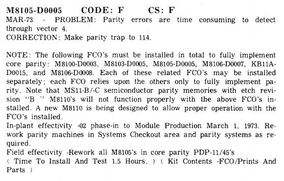
Unfortunately, no cut/jump list here (some log entries do contain these). There is a bunch of useful info to be gleaned, though:
-
The complete trap parity to 114 mod involved all of the M8100 (DAP), M8103 (RAC), M8105 (TMC), M8106 (UBC) boards, plus mods to the processor wire-wrap backplane.
-
All of these FCOs are given prefix "D", meaning DEC viewed fixing these in the field as "low priority".
-
A reason for the change is given: "Parity errors are time consuming to detect..." I suppose what they mean is that adding code to sniff for possible parity errors, in order to distinguish these from other possible sources of trap 4, was getting in the way of handling the other trap 4 sources promptly. I can't see that there would be any difference in processor overhead per se in dispatching between vector 4 and vector 114?
-
Machines which would trap parity to 114 as-delivered were phased into production starting in March 1973. This is consistent with the low serial number and component date codes in my machine, confirming its manufacture somewhere in 1972.
-
The note about the MS11-B/C (M8110 SMC) is also interesting, in conjunction with fact that the re-work is called out for "all core-parity PDP-11/45's".
PDP-11/45 11/50 MOS Memory Troubleshooting Guide
As it turns out, this document is a bit of a gold mine, containing a complete list of ECO's for the '11/45 CPU/MMU/FPU modules, console, and backplane, as of 1974. There are brief notes, dates, and revision codes for each.
In the case of the M8105, we can compare this with the DEC-O-LOG we do have on bitsavers. This shows that the "Notes" in the troubleshooting guide in some cases give information not included in the corresponding DEC-O-LOG entries. For example, the DEC-O-LOG entry for M8105-00002 says only:
Change disable gate in priority arbitration.
...while the troubleshooting guide offers a bit more explanation:
Corrects FP TRAPS to location 4 where BRs below 7 occur at the same time.
The troubleshooting guide also calls out several "clusters" of interdependent ECOs:
-
Parity, as remarked above: M8100-00003, M8103-00005, M8105-00005, M8106-00007/00008/00012/00012A, KB11-A-00015, and M8110-00018.
Separately, M8106-00003, from August 1972, is annotated "Adds disable jumper for UNIBUS PARITY", as observed missing in my hardware in the previous article.
-
CMP.B, BIT.B: M8100-00002A, KB11-A-00006. These are dated June, 1972. Hmm, I should check these instructions on my machine...
-
Speed-up: M8104-00002, M8106-00005A, KB11-A-00012A/00013. Not sure what is "sped up" here, but perhaps Unibus signaling; the M8106 change is annotated "Clear MSYN with T1".
Also of note are a few items that seem to relate directly to previously observed behaviors of my machine:
-
KM11 uPB: M8109-00015 "CPU fails to halt on selected ROM state when micro program break mode is set on maintenance card. Detected when running a test sequence not containing a pause, i.e., 150ns cycle time." Ah ha! I had run across this (mis)behavior previously, noted here.
-
Slots 26-28: KB11-A-0008 "Signal missing in small peripheral controller slots in KB11-A (slots 26-28)." Another ah ha... This seems likely related to issues noted here.
-
Burnt +5V Trace: KB11-00001: "Reworks backpanels with 24 AWG wire in parallel with +5 V etch." This may explain the burnt trace and "extra red wire" as noted here.
Jay Jaeger DEC-O-LOG Microfiche Transcriptions
After an ask on the cctalk mailing list, Jay Jaeger commented that he has some complete sets of DEC-O-LOGs on microfiche! Though he has no equipment with which to scan fiche, he very kindly took the time to manually transcribe those that seemed like they might be of most interest to me (thanks, Jay!) Jay has made his transcriptions publicly available here, under pdf/dec/fieldService/dec-o-log.
There is a lot there, and it's worth a read. Here are some excerpts I found relevant to discussions and investigations here:
-
On the parity rework:
M8100-C0003 CODE: F CS C Etch C JAN-73 [FCO]
Problem: Parity errors require the generation of trap vector 114
Correction: Modify trap vector logic
Required on all 11/45 systems with parityM8103-C0005 CODE: F CS F MAR-73 [FCO]
Problem: Parity errors need special abort logic to assert ZAP signal
Correction: Modify ZAP gate on RACAM8105-D0005 CODE: F CS F MAR-73 [FCO]
Parity errors are time consuming to detect through vector 4. Core parity requires these changes: M8100-D0003, M8103-D0005, M8105-D0005, M8106-D0007, KB11A-D0015 and M8106-D0008
FCO's may be installed separately - each FCO relies upon the others only to fully implement parity.
NOTE: MS11-B/C semiconductor parity memories with etch revision B M8110s will NOT function properly with these FCOs. A new M8110 is being designed to function with these FCOs.
M8106-D0007 CODE: F CS: J [FCO]
Problem: Parity errors are time consuming to detect through vector 4
Correction Allow processor to trap to 114 for parity errors.M8106-D0008 CODE: F CS: K MAR-73 [FCO]
Problem: UNIBUS parity errors cause machine to halt
Correction: Disable UBCB UNI PERF [ 1 ] L from generating UBCB PARITY ERR SET L.M8106-C0012 CODE: F CS: M JUN-73 [FCO]
Problem: MOS Parity memory is too tight
Correction: Strobe parity errors sooner
NOTE: See M8106-C0012ARework in parity systems with M7259 or etch revision C M8110s, rework all systems with parity and all PDP11-45s at next PM.
M8106-C0012A CODE: F JUN-73 [FCO]
The rework procedure in M8106-C0012 in steps #25 and #26 incorrectly references an R22. Should be R20.
KB11A-D0015 CODE: F DD:M WL:L [FCO] MAR-73
Problem: Detection of parity errors through vector 4 is slow.
Correction: Detect parity errors through vector 114.Wire Adds: D11D2 to A06P1, E12A1 to F11F1, C09K1 to E12A1
NOTE: This FCO must be installed in conjunction with the following FCOs to implement core parity: M8100-D0003, M8103-D0005, M8106-D0007 and M8106-D0008. Each of these related FCOs may be installed separately.
Note that MS11-B/C semiconductor parity memories with etch revision B M8110s will NOT function properly when above FCOs are installed. A new M8110 is being designed to function with these FCOs.
Okay, much of this confirms deductions worked out in the previous article. The big additional clue here is that we actually have the backplane wire adds this time!
-
D11D2 to A06P1: This forwards UBCB PARITY ERR L, already at the TMC card, on to DAPE E7. This provides parity condition input to the extended trap vector generation logic explored in the previous article.
-
E12A1 to F11F1 and C09K1 to E12A1: These relate to enhanced abort processing -- they distribute UBCB PE ABORT L to TMCC E87, TMCE E38, and RACA E52, which I have not previously inspected.
Looking at the RAC changes first, we have this:
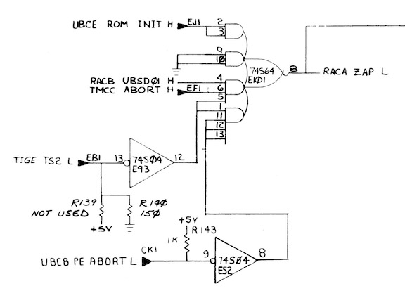
...which, per expectation, is not implemented on the RAC board I am running; no connection from CK1 to E52, and no connection from E52 to E101. The ZAP signal is used to force the microcode counter to 200 on a trap or on power up, kicking off the exception handling microcode flow on sheet FLOWS 12. I'm not sure why parity required special plumbing here; by my read a parity error should end up setting TMCC ABORT H which should also result in a ZAP?. My guess would be the special plumbing allows the trap to be taken at an earlier clock phase?
On the TMC we have these:

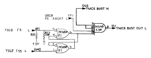
Also related to abort signaling, and also not implemented on my machine (no connection from FF1 to E87 or E38, pins 12 and 10 common on E38). So perhaps the reason to move parity to its own trap vector wasn't to avoid extra discrimintation logic in the trap 4 handler, but rather to enable an accelerated abort path without affecting extablished behavior of the other machine exceptions on vector 4? Curious...
-
-
On CMP.B, BIT.B:
M8100-A002A CODE: DF JUN-72 [FCO]
Problem: Disposition code on M8100-A0002 is 02: phase-in
Correction: Change to code 03: rework immediately.
Problem: CMP.B and BIT.B instructions with SM0 and DM0 and DF7 will destroy the PC
Correction: Inhibit PCB clock under those conditionsThe troubleshooting guide mentions that that this change also needs KB11-A-00006, but that is not included in Jay's transcript (bummer).
In any case, the description here tells us a lot more about the exact nature of the bug.
SM0,DM0,DF7here are microcode conditions; collectively this description implicates a CMP or BIT instruction, either byte or word length, with two registers as arguments, and the second argument being the PC (R7).CMP or BIT should not modify their second argument, but inspection of the the microcode flows shows that under this particular set of conditions the flow (
FET.00,FET.10,IRD.00,EXC.90) is shared with many other E/class instructions which should do. So an update inhibit derived from existing microcode outputs to distinguish this particular set of conditions is needed, and thus this FCO.Here again the schematics hold some clues. The relevant bit is the net for CLKPCB H on drawing DAPJ:

The AND terms of E42 serve as inhibits for the update signal, which otherwise sources from TIGC T1 H via E43. The top three terms in the diagram inhibit on cases of
UPCB=2 * ~SF7,UPCB=0, orUPCB=3 * ~DF7(with some term elimination on the first case). This would be the vanilla implementation of the UPCB microcode signals.The bottom-most AND term seems to be the one involved in the FCO. This adds an additional inhibit,
UPCB=3 * ICLASS * UPWE, which would be active in the situation described in the FCO description. Some minor additional clues here are that the handwriting for the signal names here doesn't quite match the rest of the drawing and that the backplane pin assignment for bringing in UPWE00 is not contiguous with the others in this net; together these suggest revision. From this we could also guess that the missing corresponding KB11-A-00006 probably involves bringing signal RACB UPWE00 H to pin E06V2.Inspection of my DAP modules shows the predicted changes implemented around E42 with green-wires, so it looks like my machine did get this FCO, either in the factory or the field:
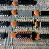
Next time I have the machine fired up I'll experiment with some BIT instructions from the front panel and make sure.
-
On the "speedup" fixes:
M8106-A0005 CODE: F CS: F DEC-72 [FCO]
Problem: Present board not meeting cycle time specifications for UNIBUS.
Correction: Add logic changes.
NOTE: This FCO must be installed in conjunction with FCO KB11A-A0012M8106-A005A CODE: F JAN-73 [FCO]
Problem 1: Rework procedure in M8106-A0005 is incorrect.
Correction 1:
In step #2 changed E83-11 to E83-13
In step #4 change R23 to R22
Problem 2: The assembly hole drawing does not specify which side of the board etch cut #13 is on
Correction 2: Side 2KB11A-A0012 CODE: F DD: J WL: J DEC-72 [FCO]
Problem: 11/45 processor does not meet UNIBUS cycle time specification.
Correction: Correct KB11-A back panel attached ADD/DELETE sheet and install FCO M8106-A0005 to UBC module.KB11A-A012A CODE: F DEC-72 [FCO]
Problem: Not all the add/deletes listed on sheet 2 of KB11A-A0012 are necessary for this retrofit.
Correction: use the ADD/DELETE sheet included in this supplement for FCO KB11A-A0012.KB11A-E0013 CODE: F DD: K WL: K JAN-73 [FCO]
Problem: Improve performance of PDP-11/45 processor as UNIBUS master.
Correction: Revise KB11-A Wire List as defined the ADD/DELETE sheet and install etch revision C M8104 moduleNOTE: This FCO completes the total FCO package necessary for improving the speed performance of the PDP-11/45 with core memory. Note prerequisite FCOs are KB11A-A0012, KB11A-A012A and M8106-A0005.
Well, definitely Unibus timing related then. There is not very much info to start from here, and logs for the M8104 module are also missing from Jay's transcripts (perhaps not issued since no F-coded ECOs for this board?)
We do see from above, though:
- Involvement of M8106 E83 (sheet UBCB, driving CLR DESKEW L). Handwriting and "white out" artifacts around this gate on the engineering drawings also suggest rework.
- Involvement of M8106 R22 (also sheet UBCB, pull up on fastbus parity error handling)
- The troubleshooting guide annotates M8106 00005 "CLR MSYN with T1". Handwriting mismatch on the clock input of the MSYN flip-flop (sheet UBCB, E79) may be related.
- At least 13 etch cuts existed in the FCO (!)
Looking through the drawings a bit more here after this, I noticed for the first time (doh!) that there is an updated set of Unibus timing diagrams explicitly to be used with M8104 rev C and post- KB11-A-E00013. The differences seem to be around the bus long pause cycle. This prompted another look through the 1972 and 1976 KB11-A maintenance manual, and sure enough, in section 8.7.2 of the 1976 version we find:
ECO KBl l-A No. 13 ("Speed-up ECO"), in conjunction with Revision C or higher of the PDR Module (M8104), has changed the data transfer operations. Explanations of both versions are presented in this paragraph. (In general, ECO KB11-A No. 13 eliminated the bus long pause cycle.)
...followed by much description of the signalling differences between pre- and post- KB11-A-E00013 machines. This can definitely be mined for further clues.
I did verify that at least some of this rework is not implemented on my M8106 boards (specifically, configuration of E83 on my boards does not match either of the apparent revisions in the drawings). Definitely a lot more work to do puzzling this one out. Even though I'll continue to investigate the details of this change, it probably ends up being too much to undertake without complete documentation.
-
On KM11 uPB Break:
M8019-C0015 CODE: F CS: R CS: M3 APR-74 [FCO]
Problem: CPU fails to halt on selected ROM state when Micro Program break mode is set on maintenance card. The problem is detected when running a test sequence not containing a pause 150 nsec cycle time. Correction: Delete U/L: CTRL latch flipflop and add latch at input gating. Test by running a branch dot with ROM match at 343.
FOR ETCH REVISION C:
Cuts:
Side 2 at E12 pin 9
Side 2 E32 pin 9 to E31 pin 13
Side 2 E32 pin 9 to E32 pin 10
Side 2 at E42 pin 13
Remove jumper E22 pin 14 to E35 pin 7Jumpers:
E12 pin 9 to E22 pin 11
E42 pin 13 to E35 pin 7
E42 pin 8 to E32 pin 9
E32 pin 10 to E31 pin 13(etch revision F instructions ellided; in Jay's transcript linked above)
NOTE: Etch revision F boards are reworked from CS revision P to R. Etch revision C boards are reworked from CS revision M2 to M3.
My M8109 timing generator is etch C. There are a lot of ECOs on this board, culminating in CS level M2 ahead of this FCO. In principle, many/most of these are verifiable by inspection, based on information contained in Jay's transcripts.
This one is a bit deep, and I haven't really covered much about the M8109 yet. I'll probably take up analysis of this problem, the associated FCO fix, and inspection/determination of the revision level of my board as its own topic in a future article. I'd like to implement this fix if it proves not overly complicated.
-
On slots 26-28:
KB11A-B0008 CODE: DF DD: E WL: E SEP-72 [FCO]
Problem: Small peripheral controller slots in KB11-A panel, slots 26 thru 28, are not wired to accept some quad module controllers: NPG, PA, PB, LTC, ACLO, DCLO and +15V are missing. Correction: Revise wiring to include signals listed above.
Wow, lots missing from these slots besides the +15V and NPG I had noticed. In other correspondence, Jay mentions that the DL11 (with which I was having trouble in these slots) is explicitly mentioned elsewhere in this FCO.
-
On the burnt-trace / extra wire situation:
KB11-00001 CODE: D May-72 [ECO]
Problem: Etch carrying +5V current from Mate-n-Lock pins to backpanel pins is not heavy enough to carry required current. Correction: Run 24AWG wire in parallel with etch on panels which already have Mat-n-Lock assembly installed. Increase thickness of conductor with solder bead if Mate-n-Lock assembly not installed. PDP-11/45 system serial number 101 and later.
Sounds about right, though the excerpt does not mention the exact trace or connector.
There are a good handful of others described in the DEC-O-LOG transcriptions as well. Probably worth making a chronological (rather than topical) pass through each of the logs and each of my boards. For another time...
Things still sought
-
Somebody to scan Jay's DEC-O-LOG fiche, so the complete contents can be made available on bitsavers. Jay kindly offered to lend these out to have them scanned. If you have the equipment for this and would be interested in helping out, please drop a line on the cctalk mailing list!
-
Information from FCO "kits", including cut/jump lists, diagrams, and instructions. I've not yet seen any of these, so I'm unsure what form they take, or where we might find them?
-
Alternate versions of the '11/45 engineering drawings. These can be quite useful for puzzling out the contents of ECOs by visually "diffing" them. So far I have only seen the June 1974 and April 1976 versions, which are currently available at bitsavers.
-
PDP-11/45 backplane wirelists. I have never seen one of these. The wirelist section in the commonly available PDP-11/45 engineering drawing sets actually describes the power harness, and not the backplane.
PDP-11/45: Parity error handling
Mon 25 May 2020 by Fritz Mueller[A catch-up article, documenting events of Jan/Feb 2019.]
At the end of the previous article, a bunch of repairs had been made to my MS11-L memory board. The associated MAINDEC diagnostic ZQMC was able to run cleanly but only with parity tests disabled. When parity tests were enabled, the parity fault LED on the MS11 would light (expected) and the machine would halt with ADRS ERR lit (unexpected...)
So the first step is to read and research how memory parity handling is implemented on the KB11-A CPU. Immediately here we run into some trouble:
-
The 1973 edition of the 11/45 Processor Handbook has a section 2.5.6, "Memory Parity", which states: "Parity errors cause the Central Processor to either trap through location 4 or to halt." There is also an Appendix E, "Memory Parity", which details CSRs for parity memory:

It is stated there that there are 16 of these, at addresses 772110-772146, each corrsponding to an 8K word block of address space.
By the 1976 version of the processor handbook, however, all of this information had been expunged. The new Appendix A, "UNIBUS Addresses", lists range 772110-772136 simply as "UNIBUS memory parity". Here, trap 4 is listed as "CPU errors", and trap 114 is listed as "Memory system errors". All subsequent revisions of the handbook state unambiguously that parity errors generate a trap 114.
-
What do the KB11-A processor maintenance manuals have to offer? Paragraph 7.7.7 of the 1972 KB11-A maintenance manual states:
A Parity error on the Unibus A is indicated by BUSA PA L high and BUSA PB L low. The parity error causes UNI PERF (Unibus parity error flag) to be set when MSYN is cleared. UNI PERF (1) L asserts UBCB PARITY ERR SET L during the pause cycle, which sets the console (CONF) flag and halts the CPU.
The semiconductor memory control EHA and EHB (enable halt) flip-flops may be set under program control to assert SMCB PE HALT if a parity error is detected. This input also asserts UBCB PARITY ERR SET L, which sets the console flag and halts the CPU. Thus, if either a Unibus A parity error or SMCB PE HALT L is asserted, the processor will be vectored to trap when the CONT switch is pressed.
Note that this text addresses how the CPU handles detected parity errors in both Unibus (first paragraph) and fastbus (second paragraph) memory systems. Unibus parity errors are stated to set the CONF flag and halt the CPU, just as I am seeing on my system... Fastbus parity handling (halt first vs. direct trap) can further be mediated by EHA and EHB, called out here to drawing SMCB in the MS11-B/C fastbus semiconductor memory print set.
But here, too, by the time we get to the later revision 1976 KB11-A,D maintenance manual, this information is revised. The updated description makes no further mention of CONF, halting, or halt control, and seems to imply that all reported parity conditions trap directly through 114.
-
How about contemporaneous memory systems? The MS11-B/C solid state memory systems released with the 11/45 (note: not what I'm running; I have the much later MS11-L) consisted of either MOS or bipolar memory matrices with an associated controller card (the M8110). These supported both Unibus and fastbus interfaces. Here, in the 1972 schematics, we see the implementation of the EHA/EHB halt control bits, mentioned above, in the upper left of sheet SMCB:
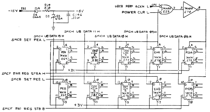
We can see the bit assignments here match the CSR layout from the 1973 processor handbook, and the associated MS11 maintenance manual from 1973 also describes them in its table 3-12:
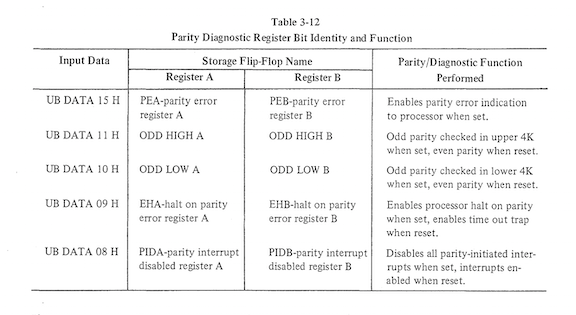
And once again, by the 1974 revision of the same maintenance manual, no surprise: descriptions of the halt control bits have been expunged from table 3-12. Okay, we're starting to get a consistent picture here...
I don't know much about the core memory systems that were configured with the early 11/45s? It would be interesting to know if anything other than the MS11-B/C ever supported this older CSR layout.
-
Let's have a look at the KB11-A engineering drawings themselves. The set I've been using during my restoration dates from 1974. The first, most obvious, place to look is trap vector generation; this is accomplished on the lower left of drawing DAPE:
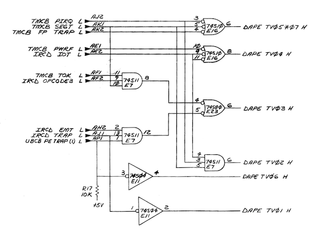
This small combinational net feeds trap vector bits to the K1MX constant multiplexer. One non-obvious wrinkle noted elsewhere on the drawing: vectors generated for reserved instruction (004), EMT (014), and TRAP (016) are further left-shifted, downstream, by microcode (state RSD.10, drawing FLOWS 12) to result in 010, 030, and 034 respectively. That's not strictly relevant to the discussion at hand, but might be helpful if pondering the logic implemented in the diagram above.
This drawing is definitely from the "post 114" era. On a parity error, we'll have ~IOT and ~PIRQ and ~SEGT, together driving TV02 high; that's our traditional vector 004. But here we also see UBCB PE TRAP (1) L, active low, entering from the left. When driven low, we'll get TV03 and TV06 high as well, all together generating vector 114.
Here we can see some clues, too, of how the change to 114 might have been bodged in: as drawn, TV01, TV02, TV03, TV04 and TV05*07 proceed nicely in order from bottom to top. But TV06, needed by the change as the most-significant "1" in "114", looks like it was just wedged in out of order on the drawing... Presumably, it makes use of a previously unused section of hex inverter E11. The change to activate TV03 here as well would have been a cut/jump at the inputs of E7.
And sure enough, here we see differences with my actual hardware! Here's part of the layout of module DAP from the '74 engineering drawings, and a snap the same corner of my DAP spare which is same as the one I'm currently running in the machine:
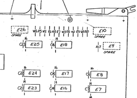
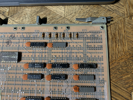
Note particulary that R17, a pullup for UBCB PE TRAP (1) L, is missing on my board. A little further work with the beeper shows that on my boards E7 pin 1 is connected directly to E7 pin 13, and is not connected to edge connector AP1. E11 pin 3 appears to be NC. Furthermore, examination of the backplane shows that there is no wire wrapped in place at DAP AP1 to deliver signal UBCB PE TRAP (1) from the UBC board. So, I think I can conclude we're not looking at a bug or component failure here; my 11/45 simply pre-dates the change from vector 4 to vector 114.
-
Okay for the vector, but what about the halt behavior? Here, the text quoted earlier from the 1972 KB11-A maintenance manual has our clue where to look. The parity derived signal eventually resulting in the halt on either Unibus or fastbus parity error is UBCB PARITY ERR SET L (note "SET" in the signal name here, don't confuse with UBCB PARITY ERR L...) The 1974 drawings imply that a fastbus parity err, but not a Unibus parity error, will halt the machine, in conflict with this text. But looking here, we see another bodge clue: the hookup at E68 pins 4 and 5 as drawn looks a little suspicious...
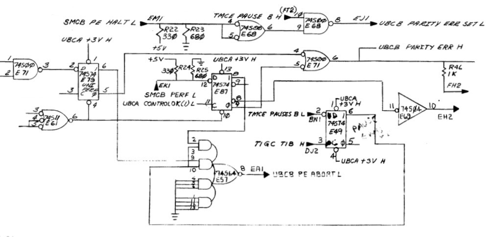
And indeed, on my hardware, E68 pins 4 and 5 are not connected together; rather, E68 pin 5 is connected to E79 (Unibus parity error flag) pin 5. So, Unibus parity errors will also halt this version of the 11/45 hardware, by design.
Some other differences related to parity are also apparent looking at my version of the UBC board. E57, seen above generating UBC PE ABORT L, is not populated. This seems related to some further refinement of abort sequencing, but the cirumstances surrounding the need for this aren't clear to me at this point. Also, jumper W1 and associated logic to entirely disable Unibus parity error detection are not present:
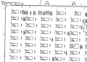
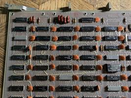
So, what does all this mean? Well, for one thing, there apparently isn't anything actually in need of repair here -- as far as I can tell, this version of the hardware is functioning per design, such as it is.
And as it turns out, with a now properly repaired MS11-L, actual parity errors are few and far between (I've yet to see any that weren't intentionally created by diagnostics.) According to Noel, stock Unix V6 doesn't do anything whatsoever with parity. RSTS/E V06C boot code seems to be properly probing and identifying the CSR on my MS11-L. And good old RT11 has seemed happy enough in the past. So I just may not need a totally up-to-date parity implementation on my machine.
There is still the issue of more broadly tracking down and implementing outstanding ECOs for this machine. I have so far had limited success in locating these (more on this next time!) I'm certainly equipped here to implement field cuts and jumps, but it might get tricky to track down newer versions of boards for any ECOs that involved total swaps to updated etches. In any case, in the absence of complete information on the ECOs I'm hesitant to cherry pick changes such as those identified here unless I am really blocked without them; better by far not to leave the machine in an undocumented "in-between" state.
Footnotes: a lot of the discovery documented here took place in the context of the enthusiast community on the cctalk mailing list, and also in private communications. Noel Chiappa and Paul Koning were both particularly generous with their time (thanks, guys!) Here are some interesting related bits that didn't fit directly in the narrative above, for completeness and for future reference:
-
On RSTS parity CSR sniffing, from Paul:
From: Paul Koning
To: cctalk
Subject: Re: PDP-11/45 RSTS/E boot problemFritz Mueller wrote:
There is a lot of inconsistent and incomplete information in the documentation about memory CSRs. They appear to come in different flavors depending on memory hardware; some of the earlier ones support setting a bit to determine whether parity errors will halt or trap the CPU, while some of the later ones (like my MS11-L) simply have "enable" and don't distinguish between halt and trap. I'm curious how OS init code sniffs out what memory CSRs there are, determines their specific flavors and, in a heterogeneous system, determines how much address space is under the auspice of each CSR? Maybe Paul and Noel can comment here wrt. RSTS and Unix respectively?
I quickly skimmed some RSTS INIT code (for V10.1). Two things observed:
1. At boot, INIT determines the memory layout. It does this by writing 0 then -2 into each location to see if it works. If it gets an NXM trap (trap to 4) or a parity trap (trap to 114) it calls that 1kW block of memory non-existent. For the case of a parity error, it tells you that it saw a parity error and is disabling that block for that reason.
2. In the DEFAULT option (curiously enough) there is a routine that looks for up to 16 parity CSRs starting at 172100. This happens on entry to the memory layout option. You can display what it finds by using the PARITY command in response to the "Table suboption" prompt.
It checks if the bits 007750 are active in the parity CSR, if so it takes that to be an address/ECC parity CSR. It figures out the CSR to memory association by going through memory in 1 kW increments, writing 3, 5 to the first 2 words, then setting "write wrong parity" in each CSR (007044), then doing BIC #3,.. BIC #5,... to those two test words, then reading them both back. This should set bad parity, and it scans all the CSRs to see which one reports an error (top bit in the CSR). If no CSR has that set, it concludes the particular block is no-parity memory.
I probably got some of the details wrong, the above is from a fast skim of the code, but hopefully it will get you started.
My machine currently has one MS11-L, which has the newer CSR layout referred to by Paul above (different than the much older MS11-B/C CSR layout depicted at the top of this article; see MS11-L docs for further details). RSTS init defaults->memory->parity on my system reports (correctly):
0K: 00000000 - 00757777 ( 124K) : 00
Presumeably, RSTS carries out this identification activity with the CSR report enable bits off, and the CSR error bits still function correctly in these circumstances; otherwise, per above, my machine would summarily halt during this process!
-
Noel, in some of his research, found Deeper magic from before the dawn of time re. evolution of the Unibus parity implementation before the era of the start of this article, bridging back to the KA11 (11/20) CPU. Quite interesting!
From: Noel Chiappa
Subject: Change in UNIBUS parity operation (Was: PDP-11/45 RSTS/E boot problem)
To: cctalkEven better, it claims to be able to control whether the memory uses odd or even parity! (How, for UNIBUS memory, I don't know - there's no way to do this over the UNIBUS.
So this really confused me, as the UNIBUS spec says parity is wholly within the slave device, and only an error signal is transferred over the bus. E.g. from the 'pdp11 peripherals handbook', 1975 edition (pg. 5-8): "PA and PB are generated by a slave ... [it] negates PA and asserts PB to indicate a parity error ... both negated indicates no parity error. [other combinations] are conditions reserved for future use."
The answer is that originally the UNIBUS parity operation was different, and that sometime around the introduction of the PDP-11/45, they changed it, which is apparently why Appendix E, about parity in the /45, says what it does!
I found the first clue in the MM11-F Core Memory Manual (DEC-11-HMFA-D - which is not online, in fact no MM11-F stuff is online, I'll have to scan it all and send it to Al); I was looking in that to see if the parity version had a CSR or not (to reply to Paul Koning), and on the subject of parity it said this: "The data bits on the bus are called BUS DPB0 and BUS DPB1." And there is nothing else on how the two parity bits are used - the clear implication is that the memory just stores them, and hands them to someone else (the master) over the bus, for actual use.
Looking further, I found proof in the "unibus interface manual" - and moreover, the details differ between the first (DEC-11-HIAA-D) and second (DEC-11-HIAB-D) editions (both of which differ from the above)!
In the first, Table 2-1 has these entries for PA and PB: "Parity Available - PA ... Indicates paritied data" and "Parity Bit - PB ... Transmits parity bit"; at the bottom of page 2-4 we find "PA indicates that the data being transferred is to use parity, and PB transmits the parity bit. Neither line is used by the KA11 processor."
(Which explains why, when, after reading about parity in the MM11-F manual, I went looking for parity stuff in the KA11 which would use it, I couldn't find it!)
In the second, Table 2-1 has these entries for PA and PB: "Parity Bit Low - PA ... Transmits parity bit, low byte" and "Parity Bit High - PB ... Transmits parity bit, high byte"; at the top of page 2-5 we find wholly different text from the above, including "These lines are used by the MP11 Parity Option in conjunction with parity memories such as the MM11-FP."
I looked online for more about the MP11, but could find nothing. I wonder if any were made?
This later version seems to agree with that Appendix E. I tried to find an early -11/45 system manual, to see if it originally shipped with MM11-F's, but couldn't locate one - does anyone have one? The ones online (e.g. EK-1145-OP-001) are much later.
It's also interesting to speculate about reasons why these changes were made; I can think of several! :-)
All for now!
PDP-11/45: V6 Unix attempts & MS11-L repairs
Mon 21 January 2019 by Fritz MuellerFollowing up on Noel's suggestion, I decided to give V6 Unix a try to see how it fared in comparison to the problems seen with RSTS/E V06C. I recently scored an additional RK05 pack from eBay, and decided to try and use that so I could keep my current RSTS/E pack intact.
Inspected the pack, and it looked in good shape, clean, with no apparent crashes on the media. Mounted it up and was able to do only a partial recovery. What I got looks like pretty generic RT-11/BASIC-11 stuff, so I'm not too concerned about attempting a complete recovery. Went ahead and reformatted the pack, after which I could read/write the entire pack with no bad sectors. So now I had two clean packs to work with.
Built a V6 Unix pack image from the Ken Wellsch tape under SIMH (using directions here). Transferred it over using PDP11GUI, and it
did boot in single-user mode. However, it immediately dumped core on the first ls command... Tried a
multi-user Unix boot (what's to lose?) and this actually fared a bit better; able to ls, but still dumped
core when trying to run the C compiler or do anything else memory-intensive.
So, all of this taken together made me (and others collaborating on the troubleshooting on cctalk) think that I might have a memory issue in the machine. My machine has a 256KB MS11-L; I had previously spot-checked this from the front panel by manipulating the KT11-C mapping registers and trying some writes/and reads within each bank. This was enough to identify and repair a few major problems (see this older blog post) and to get me this far. But I had never thoroughly and substantially beat this card up after things seemed to be working with RT-11. There was still also nagging concern that none of the heavier-weight KT11, MS11, KB11 "exerciser" MAINDEC diagnostics had yet been run to completion on the restored machine either...
The recommended DEC diagnostic for the MS11-L is ZQMC, but it is complicated, takes a long time to download, and the available sources don't exactly match the binary. So, probably better to work up my own standalone diagnostic to catch and fix obvious things... Thus followed about a week of part-time work working up and successively refining the following test code, and repairing identified problems (failed DRAMs) on the MS11-L along the way. This code maps and tests every memory location on the MS11-L, using KT11 memory management. It relocates itself so it can test the lowest physical bank as well. Tests include all-ones, all-zeros, write address to location, and a "random" data test which just uses program code test sequence:
1 2 3 4 5 6 7 8 9 10 11 12 13 14 15 16 17 18 19 20 21 22 23 24 25 26 27 28 29 30 31 32 33 34 35 36 37 38 39 40 41 42 43 44 45 46 47 48 49 50 51 52 53 54 55 56 57 58 59 60 61 62 63 64 65 66 67 68 69 70 71 72 73 74 75 76 77 78 79 80 81 82 83 84 85 86 87 88 89 90 91 92 93 94 95 96 97 98 99 100 101 102 103 104 105 106 107 108 109 110 111 112 113 114 115 116 117 118 119 120 121 122 123 124 125 126 127 128 129 130 131 132 133 134 135 136 137 138 139 140 141 142 143 144 145 146 147 148 149 150 151 152 153 154 155 156 157 158 159 160 161 162 163 164 165 166 167 168 169 170 171 172 173 174 175 176 177 178 179 180 181 182 183 184 185 186 187 188 189 190 191 192 193 194 195 196 197 198 199 200 201 202 203 204 205 206 207 208 209 210 211 212 213 214 215 216 217 218 219 220 221 222 223 224 225 226 227 228 229 230 231 232 233 234 235 236 237 238 239 240 241 242 243 244 245 246 247 248 249 | KIPDR0=172300
KIPDR1=172302
KIPDR2=172304
KIPDR3=172306
KIPDR4=172310
KIPDR5=172312
KIPDR6=172314
KIPDR7=172316
KIPAR0=172340
KIPAR1=172342
KIPAR2=172344
KIPAR3=172346
KIPAR4=172350
KIPAR5=172352
KIPAR6=172354
KIPAR7=172356
SR0=177572
XCSR=177564
XBUF=177566
.ASECT
.=1000
START:
MOV #700,SP ;INIT STACK POINTER
;----- INSTALL TRAP CATCHERS
TRPS: CLR R0 ;CURRENT VECTOR
MOV #2,R1 ;VECTOR TARGET
CLR R2 ;HALT INSTR
MOV #100,R3 ;END VECTOR
1$: MOV R1,(R0)+ ;STORE TARGET AND ADVANCE
MOV R2,(R0)+ ;STORE HALT AND ADVANCE
ADD #4,R1 ;UPDATE TARGET
SOB R3,1$ ;LOOP OVER VECTORS
;----- INIT AND ENABLE MEMORY MAPPING
INITM: MOV #IPDRS,R0 ;SRC PDR INIT TABLE
MOV #KIPDR0,R1 ;DST KIPDR0
MOV #10,R2 ;DO EIGHT PDRS
MOV (R0)+,(R1)+ ;COPY AND ADVANCE
SOB R2,.-2 ;LOOP OVER PDRS
MOV #IPARS,R0 ;SRC PAR INIT TABLE
MOV #KIPAR0,R1 ;DST KIPAR0
MOV #10,R2 ;DO EIGHT PARS
MOV (R0)+,(R1)+ ;COPY AND ADVANCE
SOB R2,.-2 ;LOOP OVER PARS
MOV #1,@#SR0 ;ENABLE MEMORY MGMT
;----- TEST 32K MS11 BANKS AT PA 100000 THRU 700000,
; RELOCATE, THEN TEST BANK AT PA 000000
DOPASS: MOV #1000,R0 ;PAR FOR PA 100000
JSR PC,DOBANK ;TEST IT
MOV #2000,R0 ;PAR FOR PA 200000
JSR PC,DOBANK ;TEST IT
MOV #3000,R0 ;PAR FOR PA 300000
JSR PC,DOBANK ;TEST IT
MOV #4000,R0 ;PAR FOR PA 400000
JSR PC,DOBANK ;TEST IT
MOV #5000,R0 ;PAR FOR PA 500000
JSR PC,DOBANK ;TEST IT
MOV #6000,R0 ;PAR FOR PA 600000
JSR PC,DOBANK ;TEST IT
MOV #7000,R0 ;PAR FOR PA 700000
JSR PC,DOBANK ;TEST IT
MOV #1000,R5 ;RELOC TARGET PA:100000
JSR PC,RELOC ;GO DO IT
MOV #0000,R0 ;PAR FOR PA 000000
JSR PC,DOBANK ;TEST IT
;----- ALL DONE WITH PASS
MOV #0000,R5 ;RELOC TARGET PA:000000
JSR PC,RELOC ;GO DO IT
CLR @#SR0 ;DISABLE MEMORY MGMT
MOV #PCOMPL,R5 ;GET PASS COMPLETE MSG
JSR PC,PRSTR ;PRINT IT
HALT ;ALL DONE
;----- MAP A SINGLE 32K BANK AT VA 20000
DOBANK: MOV #KIPAR1,R1 ;WILL MAP USING KIPAR1 THRU KIPAR4
MOV #4,R3 ;FOUR KIPARS TO SET
CMP R0,#7000 ;UNLESS WE ARE IN PA 700000 BANK...
BNE 1$ ;IF NOT, SKIP AHEAD
MOV #3,R3 ;OTHERWISE, SCALE BACK TO 3 KIPARS
1$: MOV R0,(R1)+ ;SET A KIPAR AND ADVANCE
ADD #200,R0 ;INCREMENT VALUE FOR NEXT KIPAR
SOB R3,1$ ;LOOP OVER KIPARS
;----- CALCULATE END VA
MOV #120000,R1 ;MAPPED BANK END IS VA 120000
CMP @#KIPAR1,#7000 ;UNLESS WE ARE IN PA 700000 BANK...
BNE ZEROS ;IF NOT, SKIP AHEAD
MOV #100000,R1 ;OTHERWISE, END IS VA 100000
;----- ZEROS TEST
ZEROS: CLR R2 ;EXPECTED VALUE IS 000000
MOV #20000,R0 ;START AT VA 20000
1$: MOV R2,(R0)+ ;CLEAR A WORD AND ADVANCE
CMP R0,R1 ;AT END?
BNE 1$ ;IF NOT, LOOP
MOV #20000,R0 ;START AT VA 20000
2$: TST (R0)+ ;CHECK A WORD AND ADVANCE
BEQ 3$ ;IF ZERO, SKIP AHEAD
JSR PC,PRERR ;OTHERWISE, REPORT ERROR
3$: CMP R0,R1 ;AT END?
BNE 2$ ;IF NOT, LOOP
;----- ONES TEST
ONES: MOV #177777,R2 ;EXPECTED VALUE US 177777
MOV #20000,R0 ;START AT VA 20000
1$: MOV R2,(R0)+ ;WRITE A WORD AND ADVANCE
CMP R0,R1 ;AT END?
BNE 1$ ;IF NOT, LOOP
MOV #20000,R0 ;START AT VA 20000
2$: CMP (R0)+,R2 ;CHECK A WORD AND ADVANCE
BEQ 3$ ;IF EXPECTED VALUE, SKIP AHEAD
JSR PC,PRERR ;OTHERWISE, REPORT ERROR
3$: CMP R0,R1 ;AT END?
BNE 2$ ;IF NOT, LOOP
;----- WRITE LOCATION WITH ITS VA TEST
ADDRS: MOV #20000,R0 ;START AT VA 20000
1$: MOV R0,R2 ;USE VA AS TEST VALUE
MOV R2,(R0)+ ;WRITE A WORD AND ADVANCE
CMP R0,R1 ;AT END?
BNE 1$ ;IF NOT, LOOP
MOV #20000,R0 ;START AT VA 20000
2$: MOV R0,R2 ;USE VA AS TEST VALUE
CMP (R0)+,R2 ;CHECK A WORD AND ADVANCE
BEQ 3$ ;IF EXPECTED VALUE, SKIP AHEAD
JSR PC,PRERR ;REPORT ERROR
3$: CMP R0,R1 ;AT END?
BNE 2$
;----- "RANDOM" DATA TEST (PROGRAM AS TEST DATA)
RNDM: MOV #START,R2 ;SRC: START OF PROGRAM
MOV #20000,R0 ;DST: VA 20000
1$: MOV (R2)+,(R0)+ ;WRITE A WORD AND ADVANCE
CMP R0,R1 ;AT END?
BEQ 2$ ;IF SO, SKIP AHEAD
CMP R2,#END ;TIME TO RESET SRC?
BLO 1$ ;IF NOT, GO DO ANOTHER
MOV #START,R2 ;OTHERWISE RESET SRC
BR 1$ ;AND GO DO ANOTHER
2$: MOV #START,R2 ;SRC1: START OF PROGRAM
MOV #20000,R0 ;SRC2: VA 20000
3$: CMP (R2)+,(R0)+ ;COMPARE ONE WORD AND ADVANCE
BEQ 4$ ;IF SAME, SKIP AHEAD
MOV R2,-(SP) ;SAVE SRC1
MOV -2(R2),R2 ;FETCH EXPECTED VALUE
JSR PC,PRERR ;REPORT ERROR
MOV (SP)+,R2 ;RESTORE SRC1
4$: CMP R0,R1 ;AT END?
BEQ 5$ ;IF SO, SKIP AHEAD
CMP R2,#END ;TIME TO RESET SRC1?
BLO 3$ ;IF NOT, GO DO ANOTHER
MOV #START,R2 ;OTHERWISE RESET SRC1
BR 3$ ;AND GO DO ANOTHER
5$: RTS PC ;TESTS DONE, RETURN TO CALLER
;----- RELOCATE
RELOC: MOV R5,@#KIPAR1 ;MAP VA:020000 -> PA:(R5<<6)
CLR R0 ;SRC VA:000000
MOV #20000,R1 ;DST VA:020000
MOV R1,R2 ;FULL PAGE (4K WORDS)
MOV (R0)+,(R1)+ ;COPY A WORD
SOB R2,.-2 ;LOOP UNTIL DONE
MOV R5,@#KIPAR0 ;MAP VA:000000 -> PA:(R5<<6)
MOV #RELSTR,R5 ;GET RELOCATED STRING
JSR PC,PRSTR ;PRINT IT
MOV @#KIPAR1,R5 ;GET RELOCATION TARGET
ASHC #6,R4 ;SHIFT OVER FOR PA IN R4:R5
JSR PC,PRW18 ;PRINT IT
MOV #CRLF,R5 ;GET CRLF
JSR PC,PRSTR ;PRINT IT
RTS PC ;RETURN TO CALLER
;----- REPORT AN ERROR
PRERR: MOV @#KIPAR1,R5 ;GET KIPAR FOR MAPPED BASE
ASHC #6,R4 ;SHIFT OVER FOR PA IN R4:R5
ADD R0,R5 ;ADD IN ERROR VA
ADC R4 ;CARRY IF NECESSSARY
SUB #20002,R5 ;SUB VA OFFSET AND BACK UP ONE
SBC R4 ;BORROW IF NECESSARY
JSR PC,PRW18 ;PRINT PHYSICAL ADDRESS
MOV #DELIM1,R5 ;GET DELIMITER
JSR PC,PRSTR ;PRINT IT
MOV R2,R5 ;GET EXPECTED VALUE
JSR PC,PRW16 ;PRINT IT
MOV #DELIM2,R5 ;GET DELIMETER
JSR PC,PRSTR ;PRINT IT
MOV R0,R4 ;GET ADDRESS AFTER ERROR
MOV -(R4),R5 ;BACK UP AND GET ERROR VALUE
JSR PC,PRW16 ;PRINT IT
MOV #CRLF,R5 ;GET CRLF
JSR PC,PRSTR ;PRINT IT
RTS PC ;RETURN TO CALLER
;----- PRINT SIX DIGIT OCTAL NUMBER
PRW16: CLR R4 ;CLEAR UPPER WORD
PRW18: MOV #6,R3 ;SIX DIGITS TO PRINT
ASHC #1,R4 ;SHIFT IN MSB OF LOW WORD
1$: ADD #60,R4 ;MAKE INTO ASCII DIGIT
MOV R4,@#XBUF ;PRINT IT
TSTB @#XCSR ;CHECK IF XMIT DONE
BPL .-4 ;LOOP UNTIL SO
CLR R4 ;RESET OUTPUT CHAR
ASHC #3,R4 ;SHIFT IN NEXT THREE BITS
SOB R3,1$ ;LOOP DIGITS
RTS PC ;RETURN TO CALLER
;----- PRINT NULL-TERMINATED STRING
PRSTR: MOVB (R5)+,@#XBUF ;PRINT ONE CHAR AND ADVANCE
TSTB @#XCSR ;CHECK IF XMIT DONE
BPL .-4 ;LOOP UNTIL SO
TSTB @R5 ;CHECK IF END OF STRING
BNE PRSTR ;LOOP IF NOT
RTS PC ;ELSE RETURN TO CALLER
IPDRS: .WORD 077406,077406,077406,077406
.WORD 077406,000000,000000,077406
IPARS: .WORD 000000,000200,000400,000600
.WORD 001000,000000,000000,007600
DELIM1: .ASCIZ /: / ;POST-ADDRESS DELIMETER
DELIM2: .ASCIZ / / ;POST-CRC DELIMETER
CRLF: .ASCIZ <15><12> ;LINE DELIMETER
RELSTR: .ASCIZ /RELOCATED TO PA:/
PCOMPL: .ASCIZ /PASS COMPLETED/<15><12><15><12>
END: .END START
|
The code above is the end result of quite a bit of successive refinement. Things learned along the way:
-
At first the tests consisted only of writing and checking all-ones and all-zeros to each location. This did uncover one more bank with a stuck bit at only some addresses, that my previous spot-checking had missed. Lesson: you really gotta check every byte. Removed, socketed, and replaced the implicated DRAM, and my tests passed.
-
Maybe I fixed it, so after this I invested the download time to try the the DEC ZQMC diagnostic again. It ran better than I had seen before, proceeding through a few subtests, but soon started flagging a lot of errors that my diagnostic missed. Hmmm. Inspecting the DEC code, it seemed to be writing and checking random data at the time, not just all ones an zeros. Went ahead and implemented "random" data test in my diagnostic, and it immediately started implicating the same chips. Lesson: all-ones, all-zeros isn't good enough...
-
While I was at it, I implemented an additional "write/check each byte with its virtual address" test. Interestingly, this found most, but not all of the same chips as the random data test. Lesson: all-ones, all-zeros, and address in each word isn't good enough, either; you really do gotta have that "random" data test, too. At this point, went ahead and replaced three more implicated DRAMS, and my tests once again passed clean...
-
In the meantime, I did some more code reading on the DEC diagnostic, and found that various features could be enabled/disabled via the front panel switches. With some care, the diagnostic might also be restartable without having to wait for an entire re-download, if stopped carefully and in the right place. So I spent the time to re-download, and found with experimentation that the DEC diagnostic would now pass all banks of memory cleanly, as long as parity checking was disabled. Hmm...
-
Moving back to my diagnostic, I noticed that while it ran clean now on all banks, on a fresh power-up it would usually light the parity-error LED on the MS11-L on its first pass. Subsequent passes, after every location had been written at least once, were fine. Since the MS11-L doesn't have any fancy power-up init logic, it would make sense to see this if the program read locations without writing them first, but I didn't think my code did that. Enabling parity traps let me catch it in the act, and it was happening on a
CLRinstruction that I was using to init memory! Lesson: on an 11/45,CLRis implemented like other single- operand, modifying instructions, and actually does a DATIP bus cycle from the destination before writing back a zero! So useMOVinstead ofCLRto init memory if you are worried about tripping parity errors... Cleaned this up in my code, and my diagnostic now runs clean on my machine in all circumstances without ever tripping a parity error.
So, a lot of issues found and repaired on the MS11-L. Maybe still some issues with parity error handling, which seems to be halting the machine instead of taking a trap. Figured it might be worth a shot to try the operating systems again, so mounted the respective disks and tried both, and... exact same failures in both cases! Womp, womp...
Well, might as well continue to look into the parity error handling, since some things still seem fishy there. The DEC documentation is a bit murky here; various versions of the KB11-A maintenance manual and 11/45 processor handbook say different and somewhat contradictory things; some info in earlier editions is also removed from later ones. The available engineering drawings for the relevant parts of the KB11-A CPU look to have some significant differences from the actual boards I have on hand, and there are more than a few ECO's for these boards listed as relating specifically to parity handling, but for which no other information is available. And Noel has uncovered evidence that even the Unibus signaling related to parity may have been changed by DEC around the times of the early 11/45. Could be interesting...
PDP-11/45: RSTS/E V06C attempts
Mon 07 January 2019 by Fritz MuellerOkay, back in action after replacing the failed nand at B26 in the RK11-C. MAINDEC ZRKK now passes reliably. Wish I'd been able to get to the bottom of this at the show, but it was really hard to effectively debug on the floor there while the show was in progress -- you naturally want to stop and chat with everybody who drops by to take a look, so its hard to get into a good technical flow.
Since one of the RK11-C diagnostics I needed to use writes a pack destructively, I had to sacrifice my working RT-11 pack along the way. Rather than go back to the same old RT-11 image, I figured maybe time to try something different? RSTS/E would probably be more fun with multiple terminals and the DZ11 that I have anyway, and I've never actually played around with RSTS. So decided to give that a go...
Did some poking around looking at various available versions, and V06C seemed like a pretty good starting point: it's new enough to explicitly support all of my hardware (including the DZ11 and excepting the VT100), but old enough to still have relatively modest storage requirements so I can hope to run it with the single RK05 that I currently have working. There is also complete distribution tape available at rsts.org, and a fairly complete set of documentation at bitsavers.
Spent a bit of time reading the sysgen manual, and managed to sysgen under simh and generate a bootable RK05 image for my hardware. I then transferred this image to my single working pack using PDP11GUI; this is frustratingly slow (~3 hours to write a 2.5mb pack)!! I had forgotten how bad this is. I'm not quite sure why it is as slow as it is; it shouldn't take much more than 45 minutes to push that much data through a DL11 at 9600 baud, even without compression, and the PDP-11 disk subsystem can easily keep up with that. I'm not sure if PDP11GUI is spending a lot of time turning around the serial line, or has a bunch of per-character overhead, or...? In any case, I'm motivated to do something about it; more on this some other time soon.
So, unfortunately, the RSTS image which works under simh fails to completely boot on the real hardware. It runs through the initial "Option:" menu without trouble, and upon start the RSTS light chaser runs in the data lights on the front panel. Characters are echoed on the console terminal, but it never reaches code to print the banner or prompt for the initial control file. The system appears to be in a loop reading the same section of disk repetitively, and the display register shows a continuously increasing count.
Got a lot of help from folks over on the cctalk mailing list on this one, since I'm a newbie to RSTS. Paul K. provided some useful tips:
-
RSTS displays an error count in the display register, so that's why I see an increasing count there.
-
The "fancy" idle pattern that includes both the address and data lights apparently shows up in a later release of RSTS and requires a particular sysgen option, so its not surprising that I only see the pattern in the data lights on my machine.
-
The ODT debugger may be loaded with RSTS for startup debugging by configuring it using an undocumented option in the change memory layout section of the "DEFAULT" command at the boot prompt. Enter "ODT" there, and provide a space for it in the memory map. After that, at ^P at the console will take you to the ODT prompt.
Memory allocation table:

  0K: 00000000 - 00123777 (  21K) : EXEC
 21K: 00124000 - 00213777 (  14K) : RTS (BASIC)
 35K: 00214000 - 00227777 (   3K) : ODT
 38K: 00230000 - 00757777 (  86K) : USER
124K: 00760000 - End              : NXM
-
A handy way to query the RSTS symbol table is to use the "PATCH" command at the boot prompt (one can also look through the .MAP files generated during sysgen):
Option: PA
File to patch?
Module name?
Base address? ERL
Offset address?
 Base   Offset  Old     New?
041314  000000  005267  ? ^Z
Offset address? ^Z
Base address?
-
Paul also provided this procedure for triggering a crash dump from an ODT breakpoint under RSTS:
1. Make sure crash dump is enabled (in the "default" option). Start the system. Let it run for at least one minute. (I'm not entirely sure about older versions, but I think that a crash within one minute of startup is handled differently and doesn't do all the usual dump and restart machinery.)
2. Set the data switches all UP. (In SIMH, enter "D SR 177777".)
3. Set a breakpoint.
4. When you hit the breakpoint, change the PC to 52, like this:
0B:055244
_$7/055244 52
_P(you enter only "$7/" and "52
" and "P", the rest is output from ODT.) The system will write the crashdump and then automatically restart.
5. You should now have the crash dump in [0,1]CRASH.SYS
Further experiments coordinated by Paul then led to the conclusion that an error like this could reasonably be expected to be triggered by a corrupted INIT.BAC or BASIC.RTS file. This led me to wish to verify that the disk pack contents really matched the image file I was running successfully under simh. Some standalone code to dump a CRC of every sector on the pack seemed like it would be useful in this regard, so I coded up the following:
1 2 3 4 5 6 7 8 9 10 11 12 13 14 15 16 17 18 19 20 21 22 23 24 25 26 27 28 29 30 31 32 33 34 35 36 37 38 39 40 41 42 43 44 45 46 47 48 49 50 51 52 53 54 55 56 57 58 59 60 61 62 63 64 65 66 67 68 69 70 71 72 73 74 75 76 77 78 79 80 81 82 83 84 85 86 87 88 89 90 91 92 93 94 95 96 97 98 99 100 101 102 103 104 105 106 107 108 109 110 111 112 113 114 115 116 117 118 119 120 121 122 123 124 125 126 127 128 129 130 131 | RKDS=177400
RKER=177402
RKCS=177404
RKWC=177406
RKBA=177410
RKDA=177412
XCSR=177564
XBUF=177566
.ASECT
.=1000
START:
MOV #700,SP ;INIT STACK POINTER
;----- INIT CRC LOOKUP TABLE
MOV #10041,R0 ;CRC POLYNOMIAL
MOV #CRCTBL,R1 ;LOOKUP TABLE TO FILL
ADD #1000,R1 ;START FILLING FROM END (+256 WORDS)
MOV #377,R2 ;COUNT DOWN FROM INDEX 255
L0: MOV R2,R4 ;GET COPY OF INDEX
SWAB R4 ;MOVE TO UPPER BYTE
MOV #10,R3 ;LOOP OVER EIGHT BITS OF INDEX
L1: ASL R4 ;SHIFT, MSB TO CARRY FLAG
BCC L2 ;IF MSB NOT SET SKIP AHEAD
XOR R0,R4 ;ELSE XOR IN POLYNOMIAL
L2: SOB R3,L1 ;LOOP OVER BITS
MOV R4,-(R1) ;SAVE RESULT IN LOOKUP TABLE
DEC R2 ;COUNT DOWN
BPL L0 ;LOOP OVER TABLE ENTRIES
CLR R5 ;INIT SECTOR COUNTER
;----- PRINT START OF LINE
L3: MOV R5,R0 ;GET SECTOR COUNTER
JSR PC,PRNW ;PRINT IT
MOV #DELIM1,R0 ;GET POST-SECTOR DELIMETER
JSR PC,PRNSTR ;PRINT IT
;----- READ 8 SECTORS FROM DISK
L4: MOV R5,@#RKDA ;SET START SECTOR
MOV #DBUF,@#RKBA ;SET TARGET ADDRESS
MOV #-4000,@#RKWC ;READ 8 SECTORS (2K WORDS)
MOV #5,@#RKCS ;READ + GO
TSTB @#RKCS ;CHECK RKCS RDY BIT
BPL .-4 ;LOOP IF BUSY
;----- HANDLE ERROR IF ANY
BIT #100000,@#RKCS ;CHECK FOR ERROR
BEQ L5 ;SKIP AHEAD IF NOT
MOV #ERRSTR,R0 ;POINT TO ERROR INDICATOR
JSR PC,PRNSTR ;PRINT IT
MOV @#RKER,R0 ;GET ERROR REG
JSR PC,PRNW ;PRINT IT
BR L8 ;MOVE ON TO NEXT 8 SECTORS
L5: MOV #DBUF,R4 ;POINT TO START OF DATA JUST READ
;----- RUN CRC FOR ONE SECTOR. FOR EACH INPUT BYTE CH:
; CRC = CRCTBL[((CRC >> 8) ^ CH) & 255] ^ (CRC << 8)
L6: CLR R0 ;RESET CRC
MOV #1000,R1 ;LOOP OVER ONE SECTOR (256 WORDS)
L7: MOV R0,R2 ;GET COPY OF CRC
SWAB R2 ;MOVE HIGH BYTE DOWN
MOVB (R4)+,R3 ;GET NEXT INPUT BYTE TO PROCESS
XOR R3,R2 ;XOR ONTO MUNGED CRC
BIC #177400,R2 ;MASK OFF HIGH BYTE
ASL R2 ;TIMES TWO INDEX INTO LOOKUP TABLE
MOV CRCTBL(R2),R3 ;LOOKUP VALUE
SWAB R0 ;MOVE LOW BYTE OF CRC UP
CLRB R0 ;MASK OFF THE BOTTOM
XOR R3,R0 ;XOR IN THE LOOKED UP VALUE
SOB R1,L7 ;LOOP OVER BYTES
;----- PRINT CRC, DELIMIT AND LOOP
JSR PC,PRNW ;PRINT CRC, ALREADY IN R0
CMP R4,#DBUF+10000 ;END OF DISK BUFFER?
BEQ L8 ;IF SO, EXIT LOOP
MOV #DELIM2,R0 ;ELSE POINT TO POST-CRC DELIMETER
JSR PC,PRNSTR ;PRINT IT
BR L6 ;GO DO ANOTHER SECTOR
;----- DELIMIT END OF LINE, LOOP
L8: MOV #CRLF,R0 ;POINT TO LINE DELIMETER
JSR PC,PRNSTR ;PRINT IT
ADD #10,R5 ;MOVE AHEAD 8 SECTORS
CMP R5,#11410 ;AT END OF PACK?
BLT L3 ;IF NOT, GO DO THE NEXT 8
HALT ;ALL DONE!
;----- PRINT A WORD IN OCTAL
PRNW: MOV #6,R2 ;SIX DIGITS TO PRINT
MOV R0,R1 ;MOVE OUTPUT WORD OVER TO R1
CLR R0 ;RESET OUTPUT CHAR
ASHC #1,R0 ;AND SHIFT IN MSB TO START
L9: ADD #60,R0 ;MAKE INTO ASCII DIGIT
MOV R0,@#XBUF ;PRINT IT
TSTB @#XCSR ;CHECK IF XMIT DONE
BPL .-4 ;LOOP UNTIL SO
CLR R0 ;RESET OUTPUT CHAR
ASHC #3,R0 ;SHIFT IN NEXT THREE BITS
SOB R2,L9 ;LOOP DIGITS
RTS PC ;RETURN TO CALLER
;----- PRINT A NULL-TERMINATED STRING
PRNSTR: MOVB (R0)+,@#XBUF ;PRINT ONE CHAR AND ADVANCE
TSTB @#XCSR ;CHECK IF XMIT DONE
BPL .-4 ;LOOP UNTIL SO
TSTB @R0 ;CHECK IF END OF STRING
BNE PRNSTR ;LOOP IF NOT
RTS PC ;ELSE RETURN TO CALLER
DELIM1: .ASCIZ /: / ;POST-SECTOR DELIMETER
DELIM2: .ASCIZ / / ;POST-CRC DELIMETER
CRLF: .ASCIZ <15><12> ;LINE DELIMETER
ERRSTR: .ASCIZ /ERROR: / ;ERROR INDICATOR
CRCTBL: .BLKW 400 ;CRC LOOKUP TABLE
DBUF: .BLKW 4000 ;DISK DATA BUFFER
.END START
|
Running this indicated the RSTS pack was in good shape, and not corrupt. So, maybe I have had a lurking hardware bug in my memory system (a 256KB MS11-L), which never tripped up RT-11 and so has to date gone undiagnosed?
At this point, Noel suggested on cctalk that I give Release 6 Unix a try as well, and see if it suffers similarly. Worth a shot! Out of time for now, and back to the day gig tomorrow after holiday break. Happy new year, all!
PDP-11/45 Behaving Badly
Sun 09 December 2018 by Fritz MuellerWow, a year to the day since the previous post here! Not a lot of PDP-11 work this past year, with lots of other stuff like home improvements going on, but a few things worth catching up on here.
Mainly, I got brave this past year and decided to actually rent a van and take the 11/45 out of the basement to the VCF West show at the Computer History Museum in Mountain View. This was a lot more physical work than I had anticipated. Working on this thing a piece at a time, sitting in one place in the basement, you get kind of used to it and forget how much iron it actually is... But breaking it down, loading it into a van, unloading into the show, reassembling, then reversing the whole process at the end of the show is a stark reminder, both of the size of the machine and of my advancing age, ha! A huge thank-you to my workmate Brian, who selflessly gave up a weekend, a vacation day, and some mileage on his back to give me a hand. He has already informed me that "the answer for next year is 'no'." :-)
I suppose I should have expected it, but in the course of transportation to the show something shook loose resulting in a machine that wouldn't boot RT-11 when reassembled on the show floor (stupid bumpy rental van!) So my show became a two day live-troubleshooting exhibit. This was fine, and I think a lot of folks had fun jumping in and helping with troubleshooting (thanks, all!) There was a lot of interest and reminiscence about the machine and I met a lot of nice people. Still, a little disappointing, because I really had wanted people to be able to sit down and use the machine, and also because my head ended up in the machine the whole time I really didn't get to see the rest of the show or talk to other people about their exhibits! Ah well. In the end I did cajole a successful boot out of it, 15 mins. before the show closed, so at least a couple people got to sit down and play Adventure. Placed 3rd in the restoration category :-)
So, what went wrong? At the show I managed to isolate the problem to something intermittent related to interrupts from the RK11-C controller. I was still able to boot the RKDP diagnostic pack, since its bootstrap and monitor make very conservative use of processor and device interface features. Running through the diagnostics, managed to narrow down the problem to RK11-C completion polling after overlapped seeks. I guess RT-11 makes use of this feature.
I got the machine home and reassembled, and verified that the problem was still manifesting. Then many months passed, until I found some time to dig deeper into the problem just last night. The relevant failing diagnostic is ZRKK test 37, and the output is:
DRIVE 0

RK11 DIDN'T INTRUPT AFTER SK COMPLETED
  PC     RKCS    RKER    RKDS
014476  000310  000000  004713


SCP DIDN'T SET AFTER SEEK WAS DONE
  PC   RKCS
014526  000310


RK11 DIDN'T INTRUPT AFTER SK COMPLETED
  PC     RKCS    RKER    RKDS
014476  000310  000000  004712


SCP DIDN'T SET AFTER SEEK WAS DONE
  PC   RKCS
014526  000310


TIMOUT,PC=004536
And the relevant bit of the diagnostic listing:
1 2 3 4 5 6 7 8 9 10 11 12 13 14 15 16 17 18 19 20 21 22 23 24 25 26 27 28 29 30 31 32 33 34 35 36 37 38 39 40 41 42 43 44 45 46 47 48 | 014362 2$: MOV RKVEC,R1
014366 MOV #3$,(R1)+ ;SET UP VECTOR ADRES FOR RK11 INTERUPT
014372 MOV #340,(R1) ;SET UP PSW ON INTERRUPT
014376 BIS #40,@RKDA ;ADRES CYLINDER #1
014404 MOV #111,@R0 ;SEEK, GO WITH IDE SET
014410 WAT.INT ,300 ;WAIT FOR THE DRIVE TO
;INTERRUPT AFTER ADRES WAS RECVD
;WAITING TIME= 1.4 MS FOR 11/20
;280 US FOR 11/45
;ERROR, IF INTERUPT DID NOT OCCUR
;BY NOW
014414 MOV #BADINT,@RKVEC ;RESTORE UNEXPECTED RK11 INTERRUPT
014422 MOV @R0,$REG0 ;GET RKCS
014426 ERROR 75 ;INTERRUPT DID NOT OCCUR AFTER
;SEEK WAS INITIATED WITH IDE SET
014430 BR 3$+4
014432 3$: CMP (SP)+,(SP)+ ;OK, IF RK11 INTERRUPTED TO THIS
;RESTORE STACK POINTER (FROM RK11 INTERRUPT)
014434 CMP (SP)+,(SP)+ ;RESTORE STACK POINTER (FROM
;WAT.INT)
014436 MOV #5$,@RKVEC ;SET UP NEW VECTOR ADRES FOR RK11
014444 BIT #20000,@R0 ;IS SCP CLEAR
014450 BEQ 4$ ;YES, BRANCH
014452 MOV @R0,$REG0 ;GET RKCS
014456 ERROR 76 ;SCP SET BEFORE SEEK TO LAST
;CYLINDER WAS DONE
014460 4$: WAT.INT ,56700 ;WAIT FOR DRIVE TO INTERRUPT
;AFTER SEEK WAS COMPLETED
;WAITING TIME=180 MS FOR 11/20
;36 MS FOR 11/45
014464 MOV #BADINT,@RKVEC :IT'S AN ERROR IF BY THIS TIME
;INTERRUPT HAS NOT OCCURERED
014472 JSR PC,GT3RG ;GO GET RKCS, ER, DS
014476 ERROR 77 ;RK11 DID NOT INTERRUPT AFTER SEEK (TO
;LAST CYLINDER) WAS DONE WITH IDE SET
014500 BR 5$+2
014502 5$: CMP (SP)+,(SP)+ ;OK, IF RK11 INTERUPTED TO THIS AFTER
;SEEK WAS COMPLETED. RESTORE
;STACK POINTER (FROM RK11 INTERRUPT)
014504 CMP (SP)+,(SP)+ ;RESTORE STACK POINTER (FROM
;WAT.INT)
014506 MOV #BADINT,@RKVEC ;RESTORE RK11 INTERRUPT VECTOR ADRES
;FOR UNEXPECTED INTERUTS
014514 BIT #20000,@R0 ;DID SCP BIT SET?
014520 BNE 6$ ;YES, BRANCH
014522 MOV @R0,$REG0 ;GET RKCS
014526 ERROR 53 ;SCP DID NOT SET AFTER RK11 INTERRUPTED
;INDICATING SEEK WAS
|
So, based on the fact that we don't hit error 75 from 14426 (and the fact that the previous test, #36, in this diagnostic is passing) unlike some previous issues the RK11 here is able to generate interrupts and the 11/45 CPU is fielding them. The issue seems related to the seek completion polling circuitry on the RK11.
This circuitry is described in section 3.3.2 of the RK11-C manual, and is detailed in engineering drawings D-BS-RK11-C-12, sheets 1 and 2. When a seek or reset is in progress for any drive and the IDE bit in the controller is set, the controller will poll all drives for completion when it is otherwise idle. When polling is active, a pulse train which drives a count through the polled drives should be visible at B27F2:

A quick look with the 'scope shows no joy here. This clock is initiated by signal POLL; which doesn't seem to be being asserted. Checking the origin of that signal takes us to B26 and A26:

Hmmm, one of these gates (the inverter at A26) is one that had failed and that I had repaired sometime last year... Reseated the socketed replacement on A26, reloaded the diagnostic, but still no go. Well at least it wasn't my repair job! Went ahead and pulled A26 and B26 and bench tested the gates. The 8-input nand that outputs to B26J2 does look fishy. Pulled and socketed the piece, and put a replacement and some spares on order at Jameco where I can pick them up on my way in to work tomorrow. All for now!
PDP-11/45: LA30 repair IV
Sat 09 December 2017 by Fritz MuellerReceived replacement components for the blown G380 solenoid driver channel. After this repair, all pins are firing and printing correctly. Calibrated left margin. Checked pin drive signal, which was within specifications and required no adjustment.
Went to check carriage return pulse timing calibrations, but as it turns out the G396 clock accelerator card in this LA30 has not had ECO 2 applied and therefore has no timing calibration pots. Carriage return seems to be functioning correctly and reliably after the left margin adjustment in any case.
Inspected and cleaned the M7910 interface card; it appears to be in good shape. Rejumpered the base address and interrupt vector for console operation. Slotted it into the PDP-11 in place of the DL11 I had been using up until now, and cabled up to the LA30. Booted to the M9301 monitor and then on into RT-11, and everything seems to be working fine! Here's a short video of the RT-11 boot, followed by the start of a session of Adventure:
PDP-11/45: LA30 repair III
Sat 02 December 2017 by Fritz MuellerDigging in on the flip-flops identified as potentially problematic in the previous post, found that E5 had failed. Pulled, socketed, and replaced; character generator now correctly clocks all five character columns:
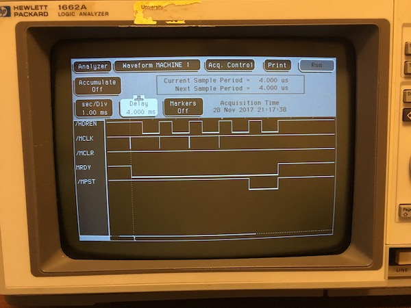
After this repair, characters were printing full width, but two problems remained: about half of the characters printed in response to typing on the keyboard were the wrong character, and the top row was not printing at all on any character:

Looking at the incorrect characters problem first, it was clear that bit 4 was not being received by the character generator correctly. I was a bit worried that the SMC KR2376-17 scanner/ROM on the keyboard assembly might be at fault, since Mattis had had some trouble with his. This is a pretty cool part; a combined scanner and code translator, with an internal oscillator, rollover logic, debounce delay, and flexible interfacing:
...not to mention the very cool vintage ceramic/gold packaging (see below.) Fortunately, inspection with an oscilloscope showed that the outputs from the scanner were just fine; chasing downstream, the problem was found to be just a loose pin (SS) on the keyboard cable Berg connector. With that sorted, we now have this:

For the final issue with the top row not printing, verified that the problem followed a particular G380 solenoid driver card when swapping them around, and that with a functional G380 in the appropriate backplane slot pin 1 fires and prints correctly. Inspection of the problematic G380 revealed a failed power transistor and blown associated micro-fuse; replacement parts on order.
For the ribbon advance issue, I pulled the ribbon motors and disassembled their top-side reduction gear cases in order to gain access to the upper rotor bearings. Cleaning and lubrication of these bearings, plus a few more taps with a mallet after reassembly, achieved an improved bearing alignment. With the increased output torque, the ribbon now advances reliably.
Other minor items: Replacement vibration isolators arrived, and were installed. Threaded inserts in the fiberglass top shell that had pulled out were reattached with epoxy.
Have some more travel coming up for work, so may not be able to get back to this for a bit. Next steps will be repair of the failed solenoid driver channel, calibrations, then any debug necessary on the M7910 interface card for the PDP-11.
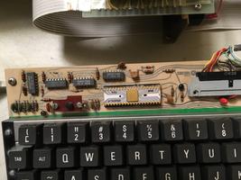
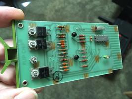
PDP-11/45: LA30 repair II
Sun 26 November 2017 by Fritz MuellerOkay, first thing to debug today is the ready light. This is lit by RDY LITE L, pin A16D2 (lower right of sheet M7721-0-1 in the LA30 engineering drawings). Logic probe showed this was correctly asserted low. Pulled the lamp and checked it with bench supply, and it checked fine. Verified +10 and ground at the lamp socket as well, so why isn't it lit? Turns out it is polarized, and the socket is soldered in backwards (?!). Corrected the socket, and ready light is working.
Noticed that ribbon is stalling occasionally. Ribbon tension seems to be overcoming the clutch on the take-up side. It seems tensioning drag on the inactive side is too high. Not sure what to do about this one yet; there is not much adjustable within the clutches, and the service manual only recommends replacement if they are out of spec (yeah, good luck finding one!)
Repeated the experiment with loopback jumper (A15R2 to A15C2). Turns out I had miscounted backplane pins the first time. With jumper placed correctly, I am now get a printing response to the keyboard. Not quite right, but definite progress:
Here I had typed :;L, and then some other letters. You can see evidence of correct pins firing for the
first three characters, though either head movement or pin timing is off. Letter spacing appears more or less
correct for 80 characters per line.
Okay, hooked up the logic analyzer, and started to take a look at the character generator clocking to see if all the the columns are being clocked out correctly. The logic analyzer shows a malfunction consistent with the print behavior: character column clocking resets after two columns rather than proceeding through all five:
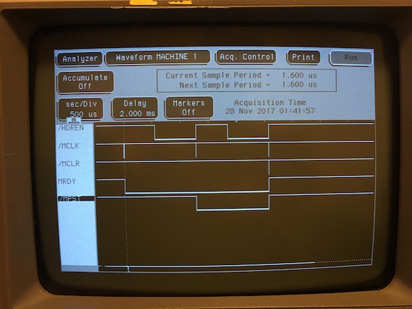
This signaling is mediated by a ripple counter on the M7724 character generator card:
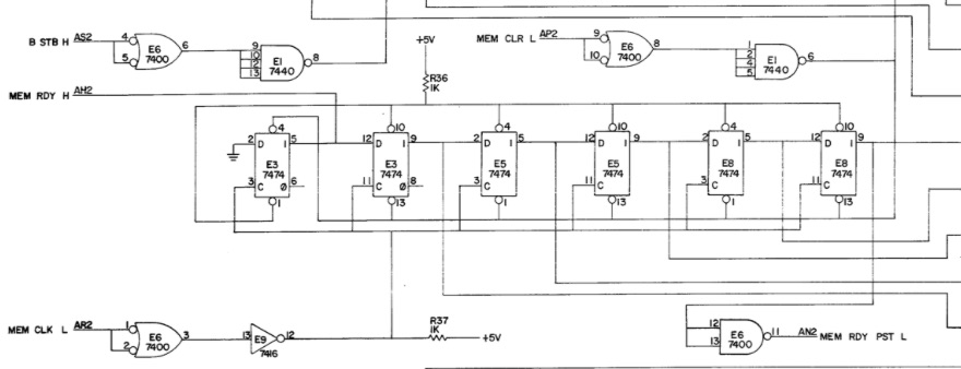
So it looks like one or more of these 7474 quad flops has failed. I note on my chargen board that these are early 70's Nat Semi parts; Mattis had a very similar issue (search "7474" on this page) on his LA30 chargen with the same parts.
All I have time for this weekend; next time I'll get the chip clip on these for a closer look, then pull and replace the baddies.
PDP-11/45: LA30 repair
Sat 25 November 2017 by Fritz MuellerOnce again its been a little while since I've had to work on PDP-11 stuff or put any updates here; the day gig has been pretty intense lately.
Recent efforts have been focused on restoration of an LA30 printing terminal. This was really filthy (including a mouse nest, yuck) so in addition to the usual electronics work it had to be completely disassembled for proper cleaning and lubrication.
First off, the H735 power supply. This is a pretty straightforward supply, but has an oil cap in the ferro- resonant circuit that is listed as a PCB-containing component; replaced this with a modern equivalent. Also pulled and reformed all the large electrolytic caps on the bench per usual. No real trouble or surprises with this supply.
Logic assembly looks good; everything is there (mine is an LA30-P, the parallel interface version) with no obvious scorches or toast. Backplane intact and chip pin corrosion doesn't look too bad. Needed some compressed air to blow out all the dust bunnies.
Print head also looks to be in decent shape; all of the pins fire freely when activated momentarily with a 15 VDC bench supply.
Most of the work here was involved in disassembling the top section of the terminal, including the keyboard and carriage assembles, where most of the filth had accumulated. There are a lot of parts and pieces, with castings, bearings, machined shafts, stainless and brass throughout. This thing was really well built!
The ribbon-like paper drag springs were all either torn, mangled, or cracked/cracking; I fashioned some replacements by cutting and drilling 1/2" x 3" strips of .002 steel shim stock. The rubber shock isolation mounts for the carriage assembly had also hardened and decayed. These look very close to the original; I put some on order. Replaced the bumpers on the carriage rails with some less expensive 3/8" chassis grommets. After cleaning, hit the slide rails with dry film silicone lubricant (Molykote 557) and pivot and carriage cam plates pins with a good lithium grease (Molykote BR2 Plus).
Ribbon drive motor bearings were very gummy, and one of the ribbon motors had seized. These motors are quite serviceable though; you can pull the bottom bearing cap and remove the rotor, clean the rotor shaft and bearings of old lubricants, apply fresh and reassemble. These are self-aligning bearings, so don't forget to give the assembly a few taps all around with a mallet after reassembly to shake them into true.
Consumables: compatible ribbons are still plentiful on eBay, so I ordered a few. Paper is an unusual width at 9-7/8". A few vendors on Amazon still seem to carry it, but it might be wise to lay in stock of a carton or two while it is still obtainable.
Fired it up after reassembly. No smoke (good!) and it feeps once reassuringly at power on. Ribbon motors and clutches seem to be working, and the ribbon advances. Activating the ribbon reverse switches manually reverses the ribbon movement per expectation.
If the carriage is closed with paper loaded, the print head will home left and then move right after about a second or so (per expectation; "last character visibility" feature) and ribbon advance halts. Local line feed from the front panel switch works. All of this indicates a good deal of the logic and the motor drive are already working correctly.
However: the front panel "ready" indicator does not light, and a quick loopback test (jumper A15R2 to A15C2 on the backplane) does not print any characters in response to the keyboard. Will pick up here with logic debug next time.
